Project update 10 of 10
Getting Started With ESP32JTAG
by Andrew LiChapter 1: Unboxing and Hardware Overview
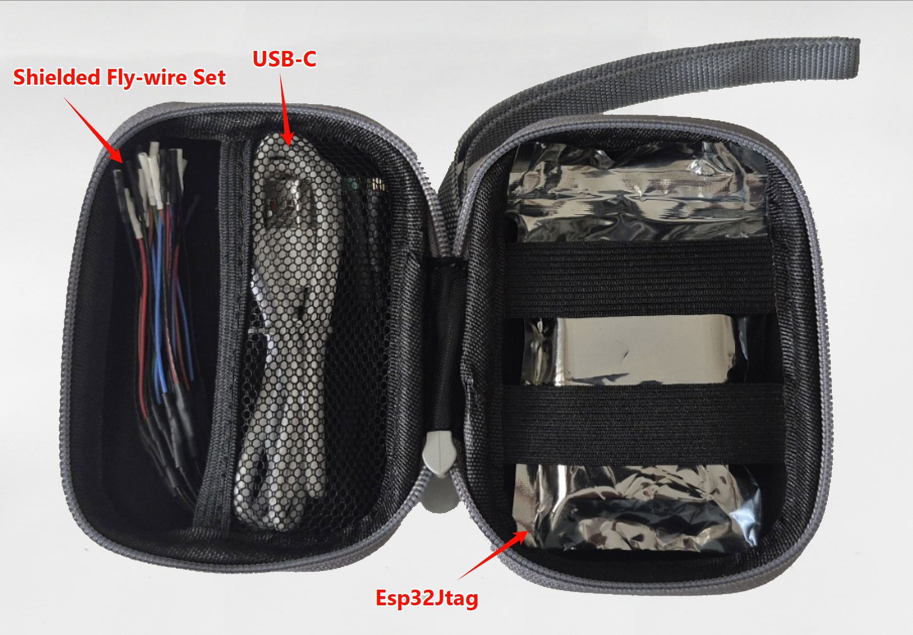
1.1 Package Contents
- ESP32JTAG host unit × 1
- USB-C cable × 1
- Port cable assemblies × 4 (each with a dedicated connector on one end and 4 color-coded flying leads on the other)
Note: No printed manual is included. This document is the primary reference.
1.2 Device Overview
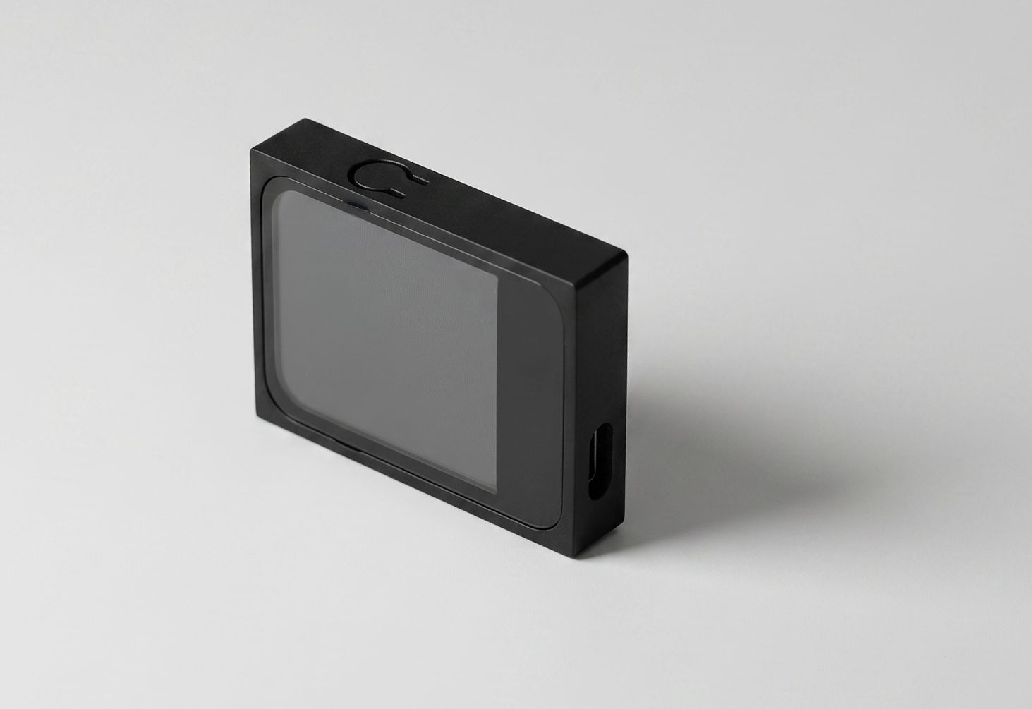
- Front: 1.83-inch LCD screen
- One side: USB-C port
- Other side: Port area
- Back: Product label
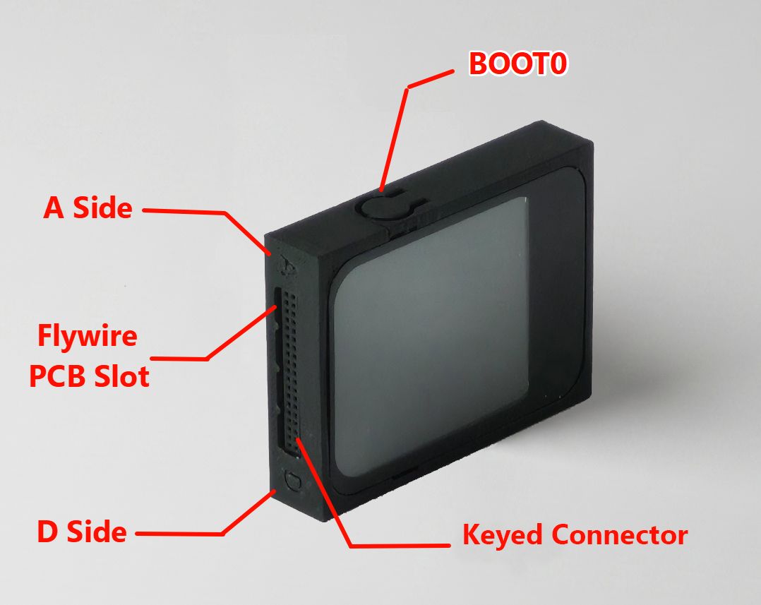
- BOOT0 / Download Mode Button: A button labeled
BOOT0is located on the top of the device. It is used to enter ROM download mode for USB wired flashing. For factory reset options, see Chapter 4.
1.3 Port Naming and Orientation
The 4 ports are located on the same side of the device, named PA, PB, PC, and PD in sequence. The housing at both ends of the port array is marked with "A" and "D" for orientation reference: the port closest to "A" is PA, the port closest to "D" is PD, and the two ports in between are PB (adjacent to PA) and PC (adjacent to PD).
1.4 Port Cable Assembly Description
Each Cable Assembly Consists of Two Parts
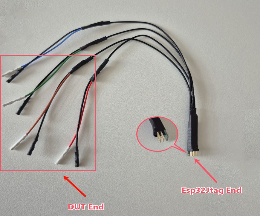
- Device end (dedicated connector): An 8-pin, 2-row dedicated connector with a keying tab on the side that mates with the PCB slot on the device (ports A/B/C/D), providing a hardware-level foolproof design that enforces a single, correct insertion orientation.
- Target board end (flying leads): Each main wire splits into two at the tip (4 pairs, 8 individual wires total):
- 4 black wires: internally connected together; carry GND to the target board in all operating modes.
- 4 color-coded wires: red, brown, green, and blue; connect to the corresponding signal pins on the target board.
Pin-to-Color Mapping for Port Connections (Quick Reference)
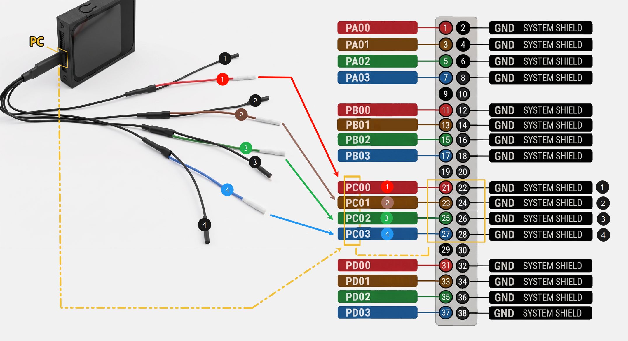
To simplify wiring, the device’s pin layout, connector key position, and flying lead colors follow a strict, absolute one-to-one correspondence. Refer to the table below when making connections:
| Wire Color | Port A | Port B | Port C | Port D |
|---|---|---|---|---|
| Red | PA00 (Pin 1) | PB00 (Pin 11) | PC00 (Pin 21) | PD00 (Pin 31) |
| Brown | PA01 (Pin 3) | PB01 (Pin 13) | PC01 (Pin 23) | PD01 (Pin 33) |
| Green | PA02 (Pin 5) | PB02 (Pin 15) | PC02 (Pin 25) | PD02 (Pin 35) |
| Blue | PA03 (Pin 7) | PB03 (Pin 17) | PC03 (Pin 27) | PD03 (Pin 37) |
| Black (×4) | GND (2/4/6/8) | GND (12/14/16/18) | GND (22/24/26/28) | GND (32/34/36/38) |
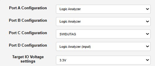
1.5 Port Modes and Pin Functions
Port Mode Quick Reference
| Port | Available Modes | Factory Default |
|---|---|---|
| PA | Logic Analyzer | Logic Analyzer |
| PB | Logic Analyzer · Vtarget + UART + SReset | Logic Analyzer |
| PC | Logic Analyzer · BMP SWD/JTAG | SWD/JTAG |
| PD | Logic Analyzer · FPGA XVC · Counter Lo @ 132 MHz · Counter Hi @ 132 MHz · GPIO Direct (125 Hz / 250 Hz / 500 Hz / 1 kHz) | Logic Analyzer |
Note: Operating modes are configured and switched through the web interface. Select the required mode before wiring or using a port.
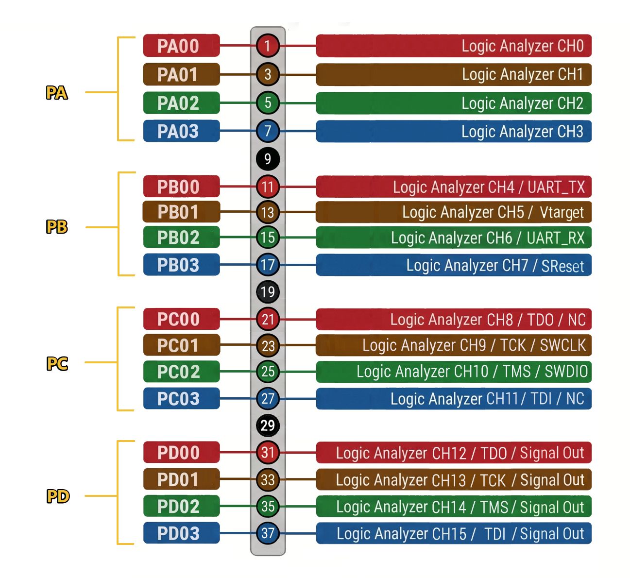
Mode 1: Logic Analyzer (supported by Port A / B / C / D)
| Pin | Wire Color | PA | PB | PC | PD |
|---|---|---|---|---|---|
| PX00 | Red | CH0 | CH4 | CH8 | CH12 |
| PX01 | Brown | CH1 | CH5 | CH9 | CH13 |
| PX02 | Green | CH2 | CH6 | CH10 | CH14 |
| PX03 | Blue | CH3 | CH7 | CH11 | CH15 |
Note:
Xrepresents the port letter A/B/C/D.
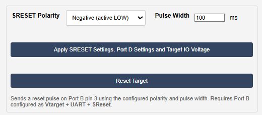
Mode 2: UART with Target Sensing & Reset Control (Port B only)
| Pin | Wire Color | Function | Description |
|---|---|---|---|
| PB00 | Red | TX | Device transmits, target receives |
| PB01 | Brown | Vtarget | Used to sense/measure the target board's voltage |
| PB02 | Green | RX | Target transmits, device receives |
| PB03 | Blue | SReset | Connected to the target board's RESET pin to manage target resets |
Mode 3: Target MCU JTAG/SWD Debugger (Port C only)
The Port C supports both JTAG and SWD interfaces for ARM Cortex MCU debugging with automatic detection (JTAG connection is attempted first, reverting to SWD if unsuccessful).
For using as JTAG port:
| Pin | Wire Color | Function | Description |
|---|---|---|---|
| PC00 | Red | TDO | Test Data Output |
| PC01 | Brown | TCK | Test Clock |
| PC02 | Green | TMS | Test Mode Select |
| PC03 | Blue | TDI | Test Data Input |
For using as SWD port:
| Pin | Wire Color | Function | Description |
|---|---|---|---|
| PC00 | Red | NC | No Connection |
| PC01 | Brown | SWCLK | Serial Wire Clock |
| PC02 | Green | SWDIO | Serial Wire Debug Data Input/Output |
| PC03 | Blue | NC | No Connection |
Mode 4: FPGA XVC (Port D only)
The Port D supports AMD (Xilinx) FPGA XVC protocol for programming and debugging via Vivado.
| Pin | Wire Color | Function | Description |
|---|---|---|---|
| PD00 | Red | TDO | Test Data Output: Receives serial data from the target FPGA |
| PD01 | Brown | TCK | Test Clock: Drives the JTAG clock signal to the FPGA |
| PD02 | Green | TMS | Test Mode Select: Controls the FPGA's JTAG state machine |
| PD03 | Blue | TDI | Test Data Input: Transmits serial data into the target FPGA |
Mode 5: Signal Generator (Port D only)
When Port D is configured as a signal generator, it functions as a signal output source for clock injection or circuit excitation. Depending on your target requirements, you can select one of the three sub-modes below.
- Sub-Mode 1: Counter Lo (High-Speed Clock Generation): Drives internal 132 MHz free-counter bits [3:0] onto Port D pins.
| Pin | Wire Color | Function | Output Frequency |
|---|---|---|---|
| PD00 | Red | Bit 0 | ~66 MHz |
| PD01 | Brown | Bit 1 | ~33 MHz |
| PD02 | Green | Bit 2 | ~16.5 MHz |
| PD03 | Blue | Bit 3 | ~8.25 MHz |
- Sub-Mode 2: Counter Hi (Low-Speed Clock Generation): Drives internal 132 MHz free-counter bits [7:4] onto Port D pins.
| Pin | Wire Color | Function | Output Frequency |
|---|---|---|---|
| PD00 | Red | Bit 4 | ~4.13 MHz |
| PD01 | Brown | Bit 5 | ~2.06 MHz |
| PD02 | Green | Bit 6 | ~1.03 MHz |
| PD03 | Blue | Bit 7 | ~0.52 MHz |
- Sub-Mode 3: GPIO Direct (Fixed Square Wave Generation): Generates synchronized, low-frequency square waves driven by the internal periodic timer. All 4 pins output the exact same synchronous signal. Wires can be mixed or connected interchangeably.
1.6 Safety Notes
Please read the following safety requirements before using this device.
Voltage limits: The recommended operating voltage range is 1.2 V–3.3 V. Each port is equipped with ESD protection to withstand transient overvoltage, but continuous input exceeding 3.3 V is not recommended.
Adjustable voltage: The target board reference voltage (VTref / VIO_VAR) is controlled by the device’s PWM output and can be configured through the web interface without requiring an external power supply.
Common ground requirement: Regardless of the operating mode, the target board GND must be connected to the ESP32JTAG via the black wire in the cable assembly.
No hot-plugging: Do not insert or remove the cable assemblies while the device or target board is powered; doing so may cause ESD damage.
Power off before wiring: It is recommended to complete all wiring with power removed, then verify all connections before applying power.
Chapter 2: Powering On and Initial Connection
The ESP32JTAG is ready to use immediately after power-on — no driver installation is required. The device automatically broadcasts a Wi-Fi hotspot, and all configuration can be completed through the built-in web interface accessed via a browser. This chapter covers how to power on the device, connect to the hotspot, and access the web interface.
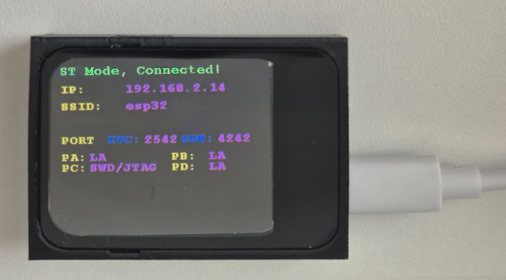
2.1 Power-On and LCD Display Overview
- Connect the device to a power source using the included USB-C cable (a computer USB port, USB charger, or power bank all work).
- The device powers on, the LCD screen lights up, and initial information is displayed:
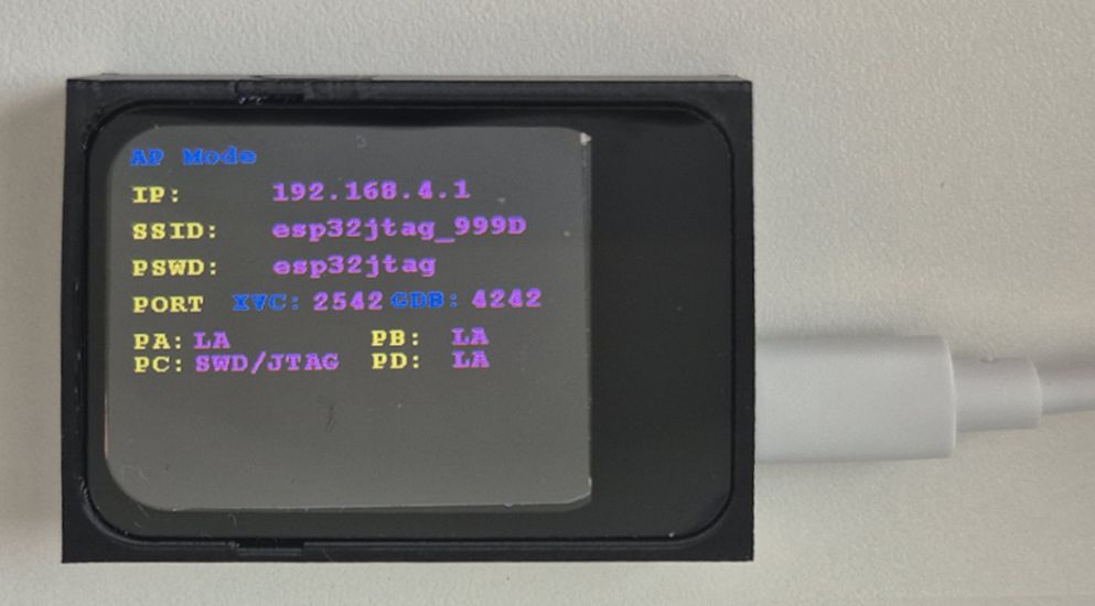
Field Descriptions
| Field | Description |
|---|---|
| AP mode | The device is currently in AP mode, acting as a Wi-Fi hotspot |
| IP | Web interface address; fixed at 192.168.4.1 in AP mode |
| SSID | Hotspot name |
| PSWD | Hotspot password |
| XVC:2542 | XVC server port, used by FPGA tools such as Vivado |
| GDB:4242 | BMP GDB server port, used by debuggers such as Cortex-Debug |
| PA / PB / PC / PD | Current operating mode of each of the four physical ports |
Note: The characters after the underscore in the SSID (
XXYY) are the "device suffix", the last 2 bytes of the device’s MAC address. The suffix is unique to each unit and is also shown on the LCD.
2.2 Connecting to the Device Hotspot (AP Mode)
- Open the Wi-Fi settings on your computer or smartphone.
- Search for the hotspot named
esp32jtag-XXYY. The device shown in the figure has the suffix 999D.
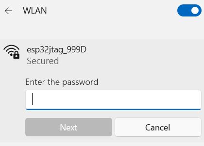
- Enter the password
esp32jtagto complete the connection.
Note: After connecting to the device hotspot, your computer will temporarily lose access to its previous network. This is expected behavior.
2.3 Accessing the Web Interface
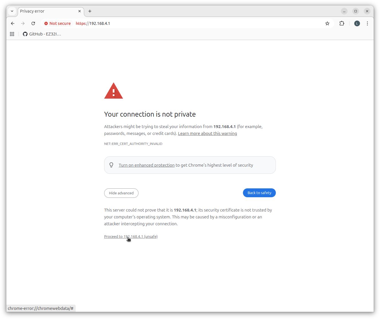
- Open a browser (Chrome, Edge, or Firefox recommended).
- Type
https://192.168.4.1in the address bar and press Enter. - The browser will display a security warning — this is because the device uses a self-signed TLS certificate and is completely normal.
Click "Advanced" → "Proceed to 192.168.4.1" (exact wording varies by browser, but the steps are the same).
- When the login prompt appears, enter the default credentials:
- Username:
admin - Password:
admin
- Username:
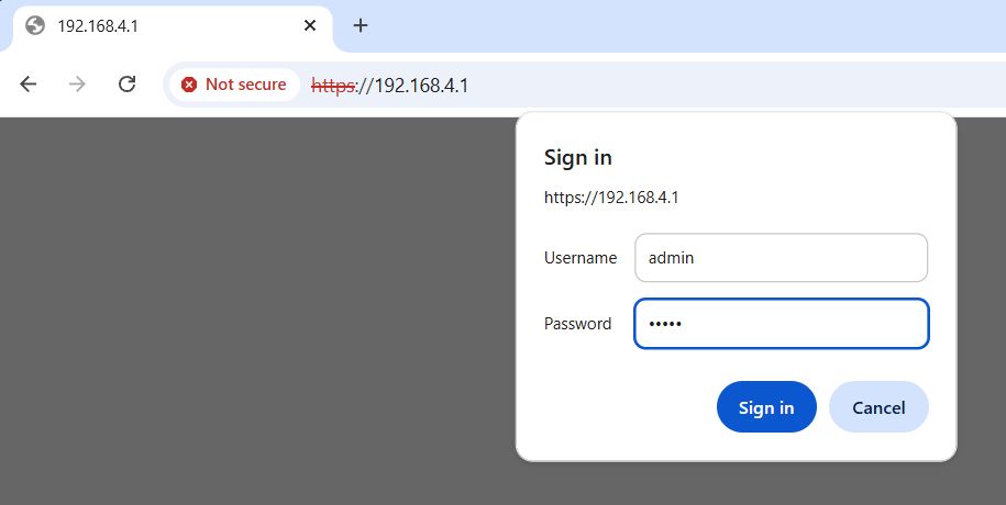
- Click
Loginto enter the main web interface.
2.4 Web Interface Overview
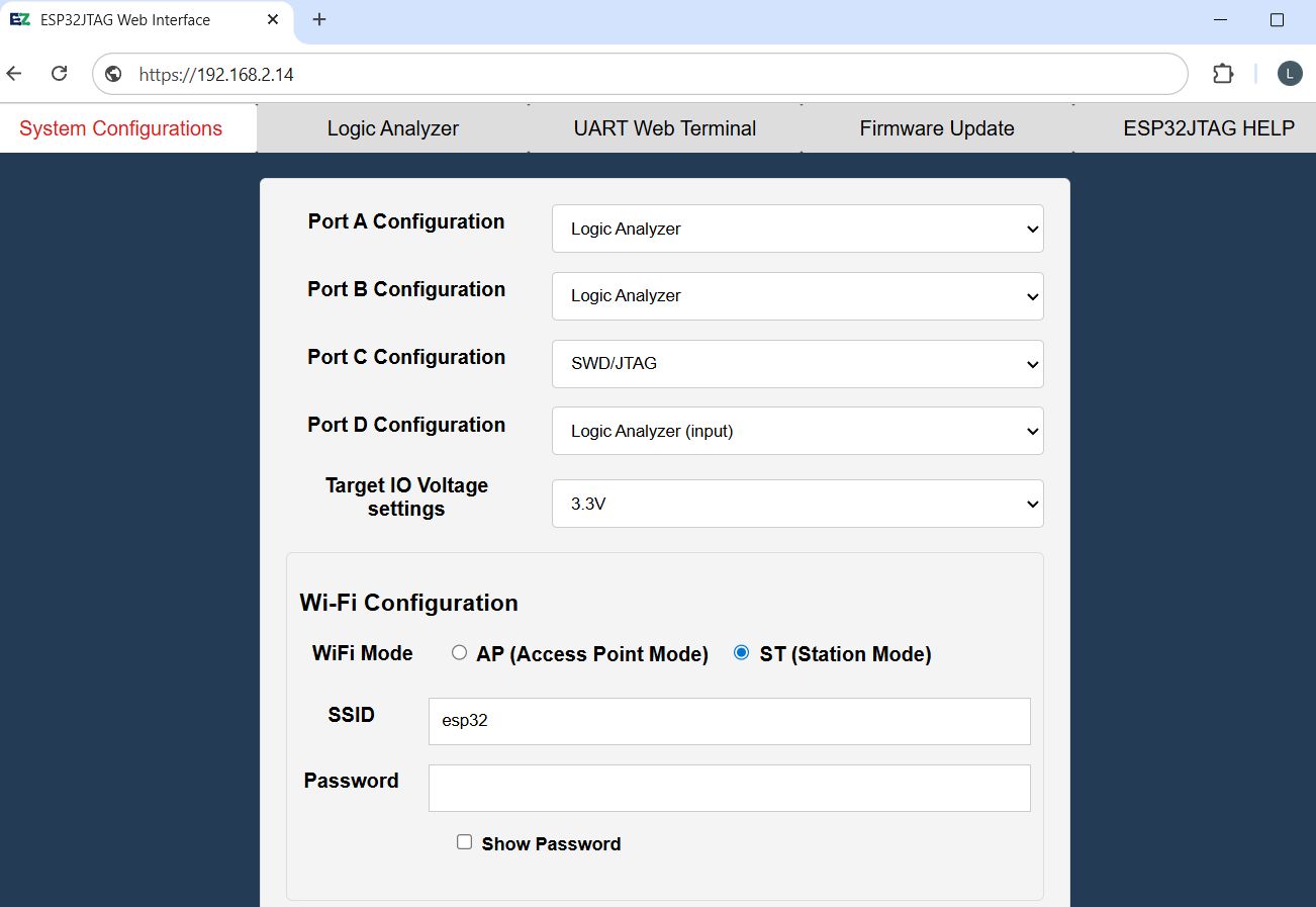
After logging in, five functional tabs are displayed at the top of the interface, providing access to all device operations.
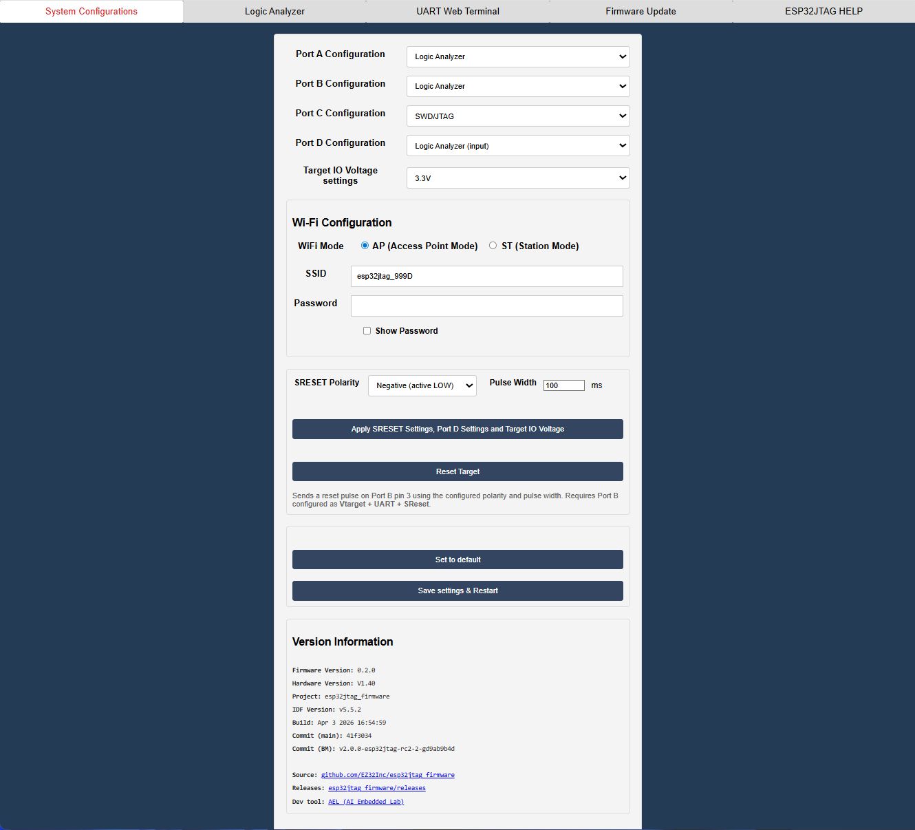
Tab Descriptions
| Tab | Description |
|---|---|
| System Configurations | Port mode configuration, Wi-Fi settings, and advanced options. Default landing page. |
| Logic Analyzer | Logic analyzer waveform capture and viewing |
| UART Web Terminal | Serial terminal for sending and receiving UART data directly from the browser |
| Firmware Update | Over-the-air (OTA) firmware upgrade |
| ESP32JTAG HELP | Built-in user guide |
Note: At this point, the device has completed its initial setup and is ready for use.
Chapter 3: Joining a Local Network (Switching to Station Mode)
By default, the ESP32JTAG operates in AP mode, which requires your computer to switch to the device’s hotspot in order to access the web interface. After switching to Station mode, the device joins your existing Wi-Fi network, allowing your computer to access it directly without changing networks — this is the recommended way to use the device on a day-to-day basis. This chapter starts from the AP mode state at the end of the previous chapter and walks through switching to and configuring Station mode.
- In the web interface, go to
System Configurations→Wi-Fi Configuration. - Select
STmode and enter the SSID and password of your local Wi-Fi network. - Click
Save settings & Restartand wait for the device to apply the configuration.
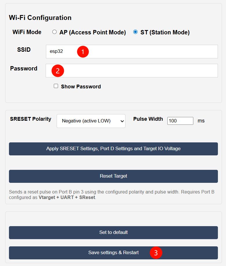
- After the device reboots, the LCD switches to show ST mode and the newly assigned IP address.
- Switch your computer back to your original Wi-Fi network, then access the web interface using the new IP address.
Note: ESP32JTAG currently supports 2.4 GHz Wi-Fi only.
If the device does not appear on your network after switching to Station mode, check the SSID and password first. If you cannot access the web interface, restore factory settings using the procedure in Chapter 4 to return the device to AP mode.
Chapter 4: Wireless Firmware Upgrade (OTA)
The ESP32JTAG supports fully wireless firmware upgrades. The entire process requires no USB cable and can be completed entirely through a browser. This chapter covers how to check the current firmware version, obtain new firmware, perform the upgrade, and recover from unexpected situations.
4.1 Checking the Current Firmware Version
Open the web interface, navigate to the System Configurations tab, and scroll to the Version Information section at the bottom of the page.
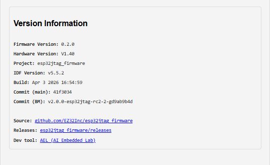
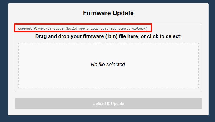
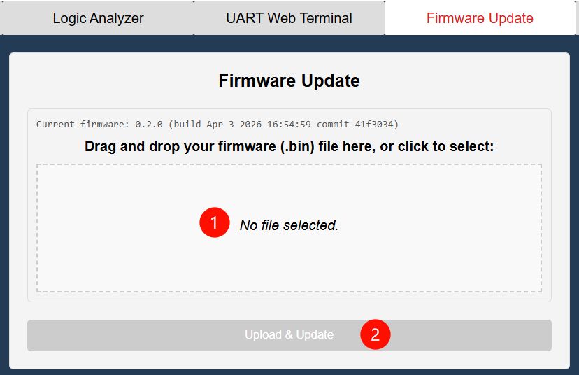
Alternatively, the top of the Firmware Update tab displays a concise summary of the current firmware (e.g., Current firmware: 0.2.0 (build Apr 3 2026 16:54:59 commit 41f3034)), making it a convenient way to confirm the version before upgrading.
4.2 Obtaining the Latest Firmware
Firmware releases are available at https://github.com/EZ32Inc/esp32jtag_firmware/releases
Each release contains two files, distinguished by their filename suffix:
| File Suffix | Purpose |
|---|---|
_ota.bin | For OTA wireless upgrades only — use this file for the procedure in this chapter |
_full.bin | Factory flashing / USB wired flashing — use only in emergency recovery scenarios |
Example filename format: esp32jtag_v0.2.0_20260403_165459_41f3034_ota.bin, which encodes the version number, build timestamp, and Git commit in sequence for easy version comparison.
Caution: Do not use
_full.binfor OTA upgrades. The OTA process only accepts_ota.bin; uploading the wrong file will cause the upgrade to fail.Note: The device does not check for updates automatically. Users must download the firmware manually and upload it themselves.
4.3 Uploading and Performing the Upgrade
- Click the
Firmware Updatetab in the top navigation bar of the web interface. - Confirm the current firmware version information shown at the top of the page.
- Drag and drop the downloaded
_ota.binfile into the dashed box in the center of the page, or click the box to manually select the file. - Click the
Upload & Updatebutton. A progress bar will appear and display the upload status in real time.
- Once the upload is complete, the device automatically finishes the upgrade and reboots.
- Reconnect to the web interface and verify that the version number has been updated in the
Version Informationsection.
Caution: Do not cut power during the upgrade process. If the upload is interrupted mid-way, the device retains the original firmware and can be safely retried.
4.4 Restoring Factory Settings
If you need to clear all configuration and restore the device to its factory state (Wi-Fi returns to AP mode, all port configurations are reset), there are two methods:
Method 1 (Recommended): Via the Web Interface
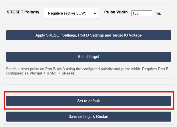
On the System Configurations page, click the Set to default button. After confirmation, the device automatically clears all configuration stored in Flash and reboots.
Method 2: USB Wired Flashing
If an OTA failure causes firmware corruption or the device enters a boot loop, the web interface will be inaccessible. In this case, recovery must be performed using the browser-based one-click flashing tool.
Use Chrome or Edge for this procedure. The WebSerial flashing tool requires Web Serial support, which is not available in Firefox or Safari. Also make sure the USB-C cable supports data, not only charging.
First, enter Download Mode by following these steps:
- Power off the device.
- Press and hold the BOOT0 button without releasing it.
- Plug in the USB cable to apply power.
- Hold for approximately 1 second, then release BOOT0.
- The LCD shows no display (black screen) → the device has entered ROM download mode. This is expected behavior.
Then, complete the browser-based one-click flashing:
- Open the following page:
https://adafruit.github.io/Adafruit_WebSerial_ESPTool/. Click the Connect button on the page.
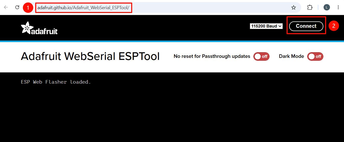
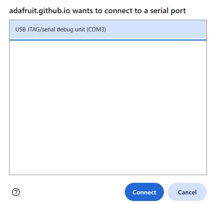
- A small browser dialog will appear (as shown below). Select your device from the list (Windows shows
COM3etc.; Mac showscu.usbserial), then clickConnect. The page will automatically detect the chip.
- Load the firmware and configure the settings:
- In the
Offsetfield, enter:0x0. - Click
Choose a fileand select youresp32jtag_vXXX_full.binfile from the dialog.
- In the
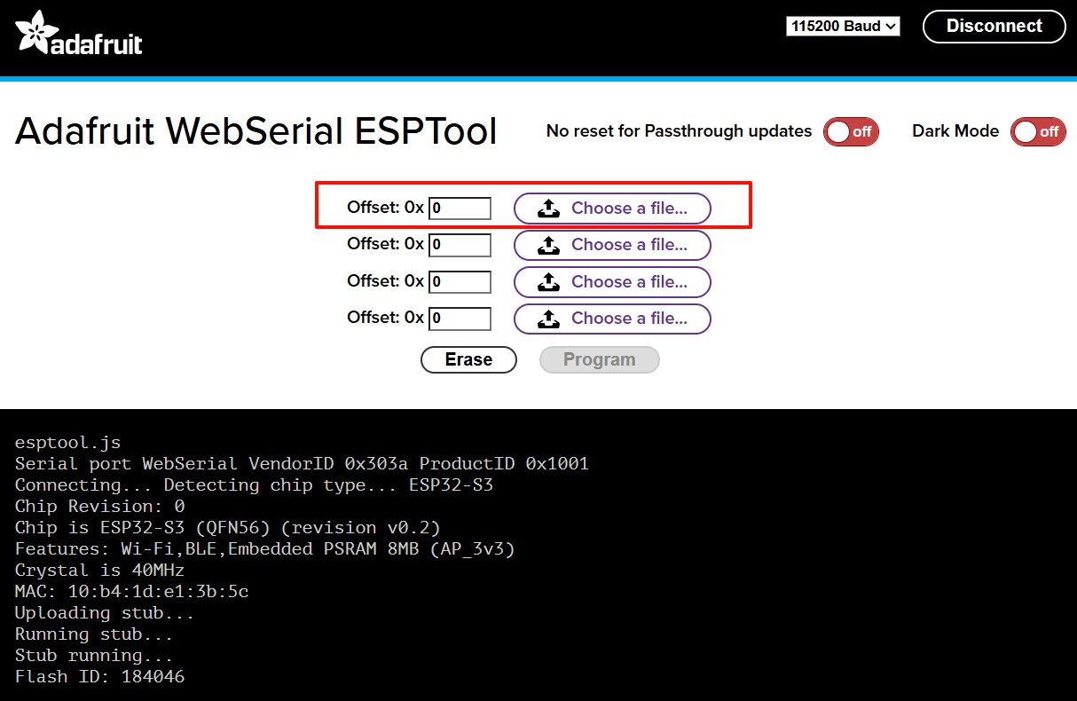
Caution: You must use the
_full.binfile here. It is a complete Flash image including the bootloader and partition table. The_ota.binfile is not valid in this mode.
- Click the
Programbutton and wait for the process to complete. - When programming finishes, unplug and reconnect the USB-C cable to reboot the device.
- Confirm that the LCD turns on and shows AP mode again.
- Reconnect to the
esp32jtag-XXYYhotspot, openhttps://192.168.4.1, and verify the firmware version in the web interface.