Project update 5 of 9
Design Deep Dive #3 - Thermal Resilience
by Sparsh BhonwalHi everyone,
Following The Efficiency Mandate, we are moving into the third technical chapter of our "Engineering Behind USB VSense" series.
It is important to note from the outset that the Gamma revision discussed here is the current production-ready version of the USB VSense. This version represents the culmination of our testing and refinement, ensuring the device is ready for high-reliability field use.
In this update, we look at how the USB VSense manages heat from two distinct sources: Joule heating (\(I^2R\)) from high-current pass-through and the heat generated by the high voltage drop across the LDO (\(P = \Delta V \cdot I\)). While the USB PD EPR standard stops at 5A, our goal for the Gamma revision was to create a device that operates with significant thermal headroom.
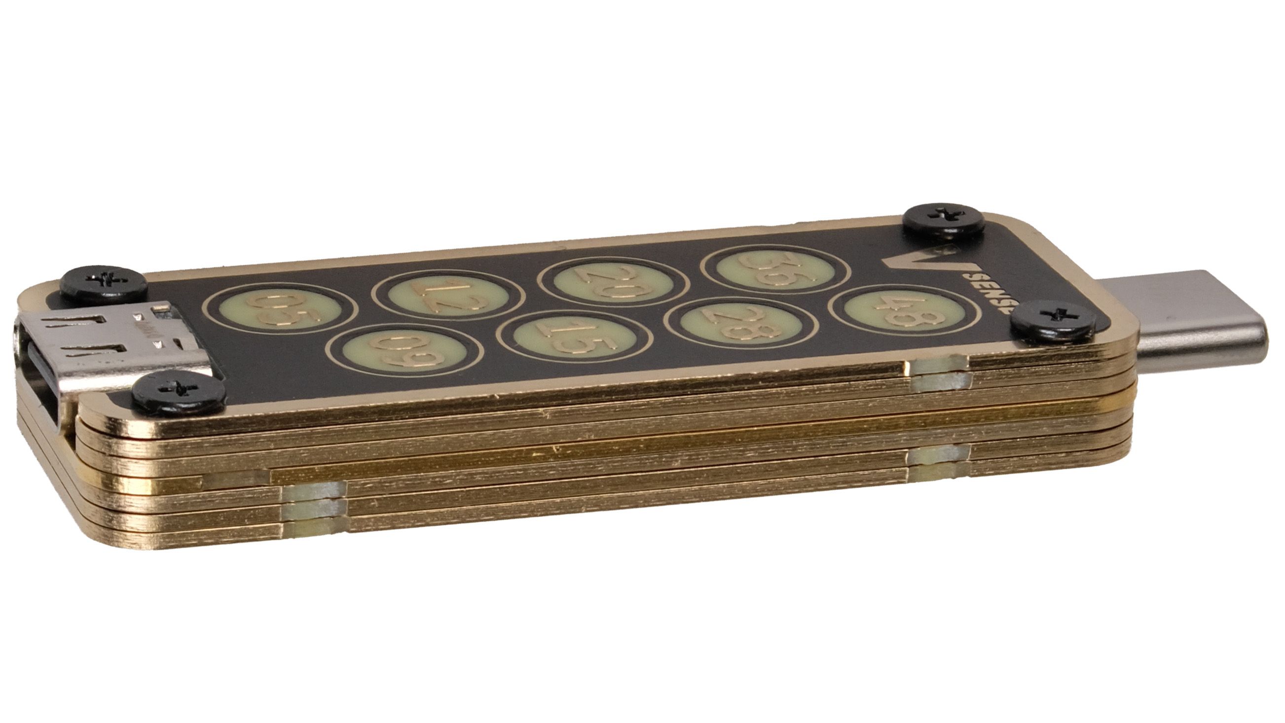
The Gamma revision represents a meticulous thermal optimization designed to turn the entire 7-PCB assembly into a unified heat sink.
1. Hardware Evolution: From Beta to Gamma
To achieve our thermal goals, we built upon the solid foundation of the Beta version and introduced three key design improvements in the Gamma revision.
Foundational Beta Features: Maximizing Current-Carrying Capacity
The Beta version utilized the Saturn PCB Toolkit as a baseline, where we doubled the numbers for extra margin—or tripled them wherever possible.
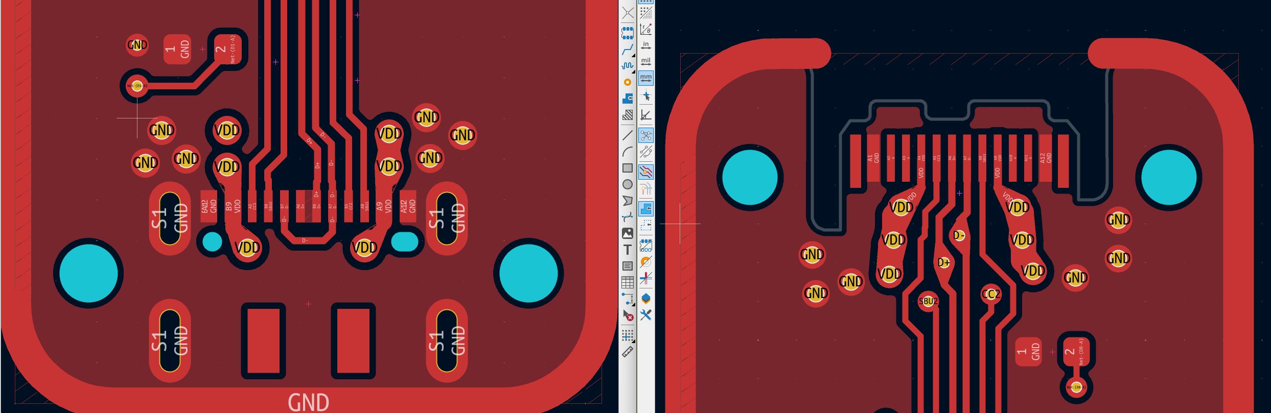
- Dedicated Layers for Power Planes: Two internal layers of the 4-layer Main PCB are dedicated strictly to power, providing massive copper volume for current flow.
- Strategic Via Placement: We optimized the high-current transitions at the connectors. While calculations showed 3 vias per connection were sufficient, we implemented 6-via arrays at both the USB-C receptacle and the USB-C plug. This ensures the shortest possible path for current to "dive" from the surface pads into the internal power planes.
Gamma Revision Improvements: Enhanced Thermal Coupling
The Gamma revision focused on extracting heat from the components and moving it to the environment more effectively:
- Pin-Level Thermal Copper Pours: We replaced standard thin traces with large copper pours for every critical LDO pin (\(V_{IN}\), \(V_{OUT}\), and \(GND\)). These "islands" act as immediate heat sinks, allowing thermal energy to spread across the surface before it is pulled into the primary ground and power planes within the PCB stack.
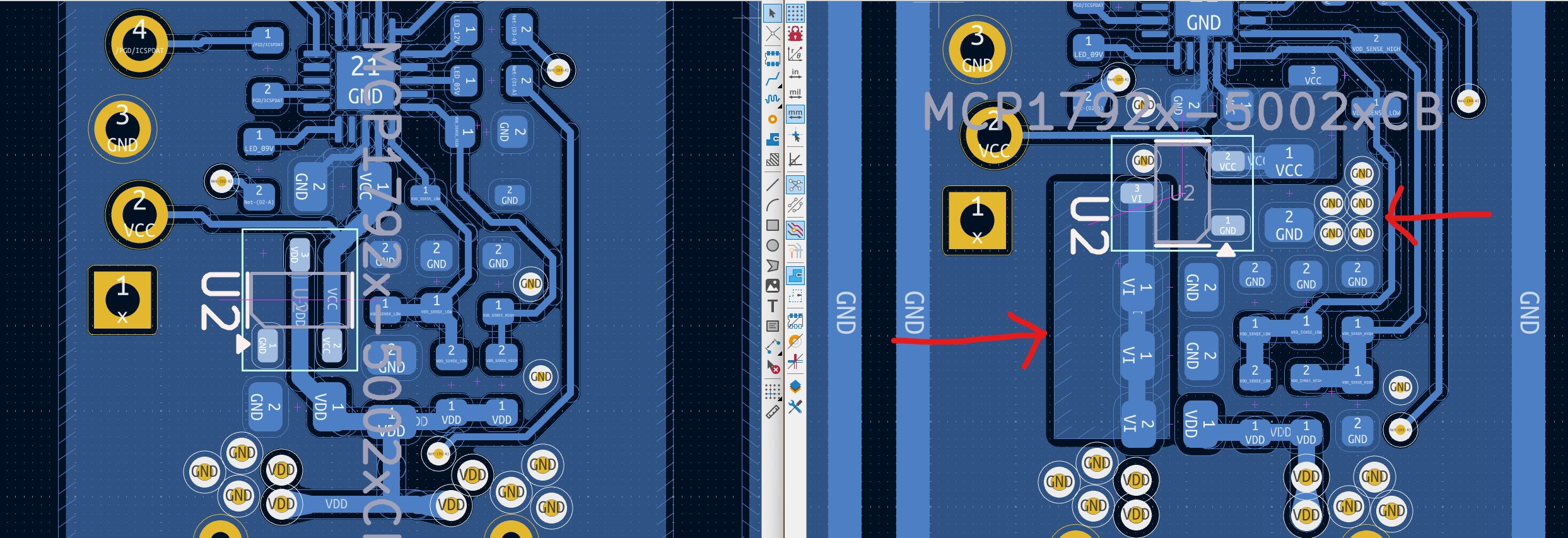
- Targeted Thermal Vias: A tight matrix of through-hole thermal vias was placed immediately adjacent to the LDO GND pin, creating a direct vertical path to pull heat into the internal ground planes.
- Side Plating (The Thermal Bridge): This is the definitive Gamma upgrade. By copper-plating the edges of all seven PCBs (the Main board and the six enclosure panels), we bypassed the fiberglass "bottleneck" of the PCB edges. This allows the Gamma revision to bridge heat from the core to the "outer shell".
2. Test Set #1: High-Current Pass-Through (The 6A Stress Test)
We pushed our steady-state testing to 6A—20% beyond the EPR 5A limit—to validate this "over-engineered" approach.
The Results (Ambient: 25.6°C | Measured with Brymen BM235):
| Test Load | Beta Main PCB | Gamma Main PCB | Improvement |
|---|---|---|---|
| 5A (EPR Standard) | 37.4°C | 36.2°C | -1.2°C |
| 6A (Stress Test) | 42.1°C | 40.6°C | -1.5°C |
Thermal imaging confirms that the Gamma PCB has no thermal epicenter. The board heats uniformly, proving the over-engineered via arrays are working as intended.
3. Test Set #2: The 55V "Time-to-Flicker" Challenge
To quantify our thermal improvements, we used the LDO’s built-in Thermal Shutdown (TSD) and Hysteresis as our measurement tool.
The LDO is designed to cut power once the silicon junction reaches its safety limit 150°C and only restarts once it cools below a specific threshold. This cycle—driven by thermal hysteresis—creates a visible flicker in the internal LEDs. By driving the LEDs to pull nearly 4x the real-world load at 55V, we measured how long the system takes to enter this thermal safety loop.
- Real-World Load (55V @ 6 mA): \(P_{D} \approx (55V - 5V) \cdot 0.006A = \mathbf{0.30W}\)
- Torture Test Load (55V @ 22.7 mA): \(P_{D} \approx (55V - 5V) \cdot 0.0227A = \mathbf{1.135W}\)
Quantifying the Thermal Bridge Performance
| Configuration | Time to Hysteresis Loop | Est. System \(R_{\theta JA}\) | % Reduction in \(R_{\theta JA}\) |
|---|---|---|---|
| Beta Main PCB (Standalone) | ~2 Seconds | ~110 °C/W | Baseline |
| Gamma Main PCB (Standalone) | 27 Seconds | ~65 °C/W | 41% Lower |
| Gamma Main PCB w/ Beta Enclosure PCBs | 60 Seconds | ~48 °C/W | 56% Lower |
| Gamma Main PCB w/ Gamma Enclosure PCBs (Side-Plated) | 100 Seconds | ~38 °C/W | 65% Lower |
The jump from 60 seconds to 100 seconds illustrates the power of Enhanced Thermal Coupling: it reduced thermal resistance by an additional ~20% simply by providing a copper-to-copper path between the boards.
Conclusion & What’s Next
By utilizing side-plating to turn the enclosure into a functional heatsink, we have effectively neutralized the thermal challenges of the USB EPR standard, while "getting away" with an LDO. The device doesn’t just survive at 48V and 5A; it stays cool and stable.
However, a device built for the field needs more than just good thermals—it needs to survive the wear and tear of hard everyday use. In our next update, Deep Dive #4: Mechanical Sturdiness, we will explore how our 7-PCB assembly is held together using SMT threads and screws to create a rugged, fully customizable chassis that allows for a complete look-and-feel change with a single panel swap.
Stay tuned!
— Team Meticulous Technologies
