Today it’s my turn to write a MNT Reform Next campaign update, and as the main electronics person at MNT, I traditionally always write one longer, more technical article during one of our campaigns. In this article, I’m going to highlight some of the technical choices behind power, charging, external displays, USB, camera, radios and PCIe.
System Controller, Power and Charging
MNT Reform Next is my second design using USB Power Delivery, building on the experience with Pocket Reform. Back then I decided against a fully monolithic solution and to retain some low-level control over PD communication so that one can do more with USB Type-C alternate modes in the future, and, as the community, learn more about the details of PD.

Power supplies and charging need to work at all times, even when the main SoC is turned off. That’s why controlling these is a job for the "System Controller", which is a small low-power processor on the motherboard. On classic Reform, this is a NXP LPC11U24, but since the Pocket Reform, I upgraded to the more capable RP2040 with dual 133 MHz ARM Cortex-M0+ cores and a well-documented C SDK. The original plan with the Next was to upgrade to the newer RP2350 series that has extra low power modes, but it’s still not possible to buy the silicon on the market, so it’s not clear if it’s going to make it into the Reform Next when we start production. I hope we’ll still be able to pull it off, though.
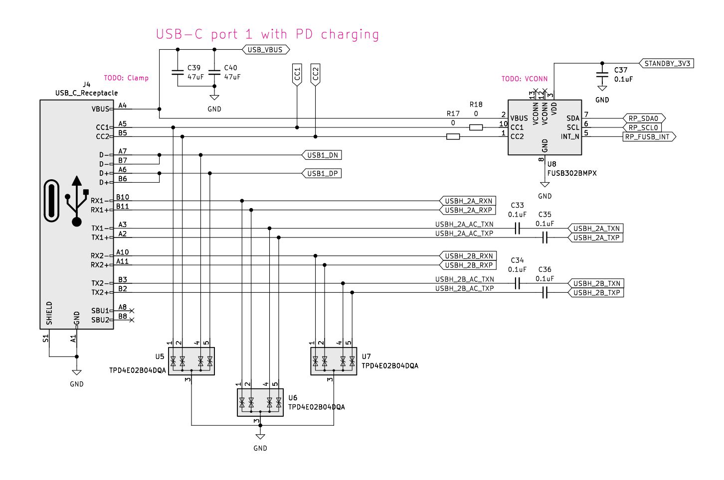
In any case, the System Controller runs our open-source C code which is organized as a state machine for the various Power Delivery states. The lowest level of USB Type-C PD communication is handled by an FUSB302B chip which is not on the motherboard itself but on the left Port Board. This separation will make it possible later to support scenarios like DisplayPort alternate mode on a different Port Board. Reusing the same RP2040 + FUSB302B combo from Pocket Reform in Reform Next allows us to build on the battle-tested Pocket Reform PD code that includes great refactoring and charger compatibility fixes by Chris Hofstaedtler and other contributors.
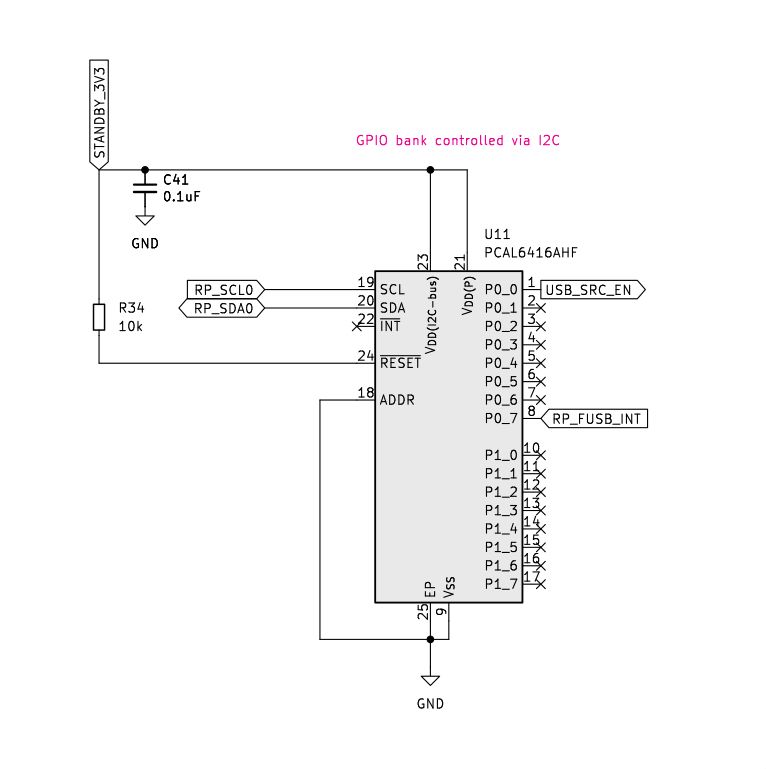
A new facet of the Next’s design is not to directly tie any off-motherboard USB- and Power-related switches to the System Controller’s GPIO lines but instead use a I2C GPIO chip that lives on the port board. This keeps the interface to the port board clean (just a I2C bus and power) and expandable.
When a power supply is connected to the USB Type-C PD port, the System Controller negotiates the best available combination of voltage and current. It prefers 20 V but can go as low as 5 V. This voltage then arrives via the VPD line of the Power Interface cable at the motherboard.

The motherboard itself features the main buck/boost switching converter, which is also responsible for controlling the charge voltage and current for the battery packs. For the Next’s completely new design I chose the modern Texas Instruments BQ25756. In contrast to the Analog/Linear LTC4020 I used on the classic MNT Reform motherboard, it has a digital control interface over I2C and can be configured by the System Controller. The BQ25756 converts the PD input voltage to the correct voltage required for charging 4 LiFePO4 battery cells in series (around 4x3.6 V = 14.4 V). Using a DIP switch, this voltage can also be switched higher in case you want to experimentally use Li-Ion cells (to 4x4.2 = 16.8 V). During beta testing it became clear that the BQ25756 is not optimal for running without batteries, as it does not have a separate power path for switching the input voltage from the wall adapter through to the system. So I’m currently working with Elen Eisendle on a new iteration with a more optimal chip.

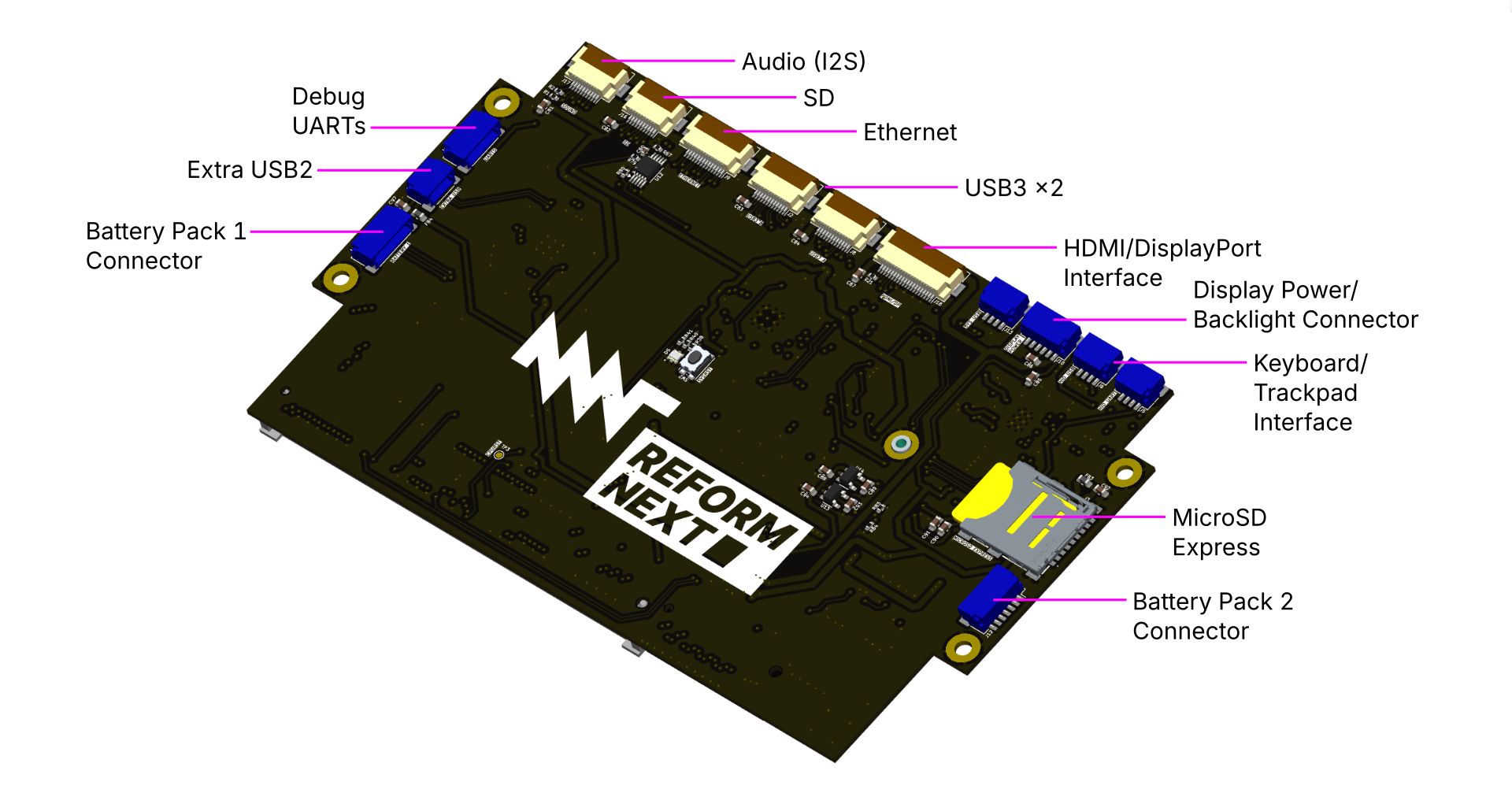
The charging voltage generated by the main buck/boost is applied downstream at the two battery pack connectors BAT1 and BAT2. I co-developed the 7-pin battery interface with Elen, who also designed the top side of the battery pack PCB. The top and bottom sides of the battery packs are PCBs with little surface mount battery contacts, and there’s a 2-pin cable to connect the two sides and close the circuit. The top PCB has the monitoring, protection and balancing functionality for the pack based on the Texas Instruments BQ76922 chip. The two packs are controlled via two different I2C buses of the System Controller to not interfere with each other. Their power input/output lines are connected together on the motherboard to allow for redundant operation. In theory, you could hot swap one pack while the laptop is running or, more practically, run on one pack if the other fails.
Displays and USB
Since the arrival of USB Type-C and alternate modes, USB, power and display technologies are hard to cleanly separate. As we don’t want to design the laptop only around a specific processor/SoC, I wanted to stay flexible in terms of future possibilities for USB Type-C ports (also anticipating USB 4) and not tie the design to the built-in USB Type-C functionality of the RK3588 SoC.
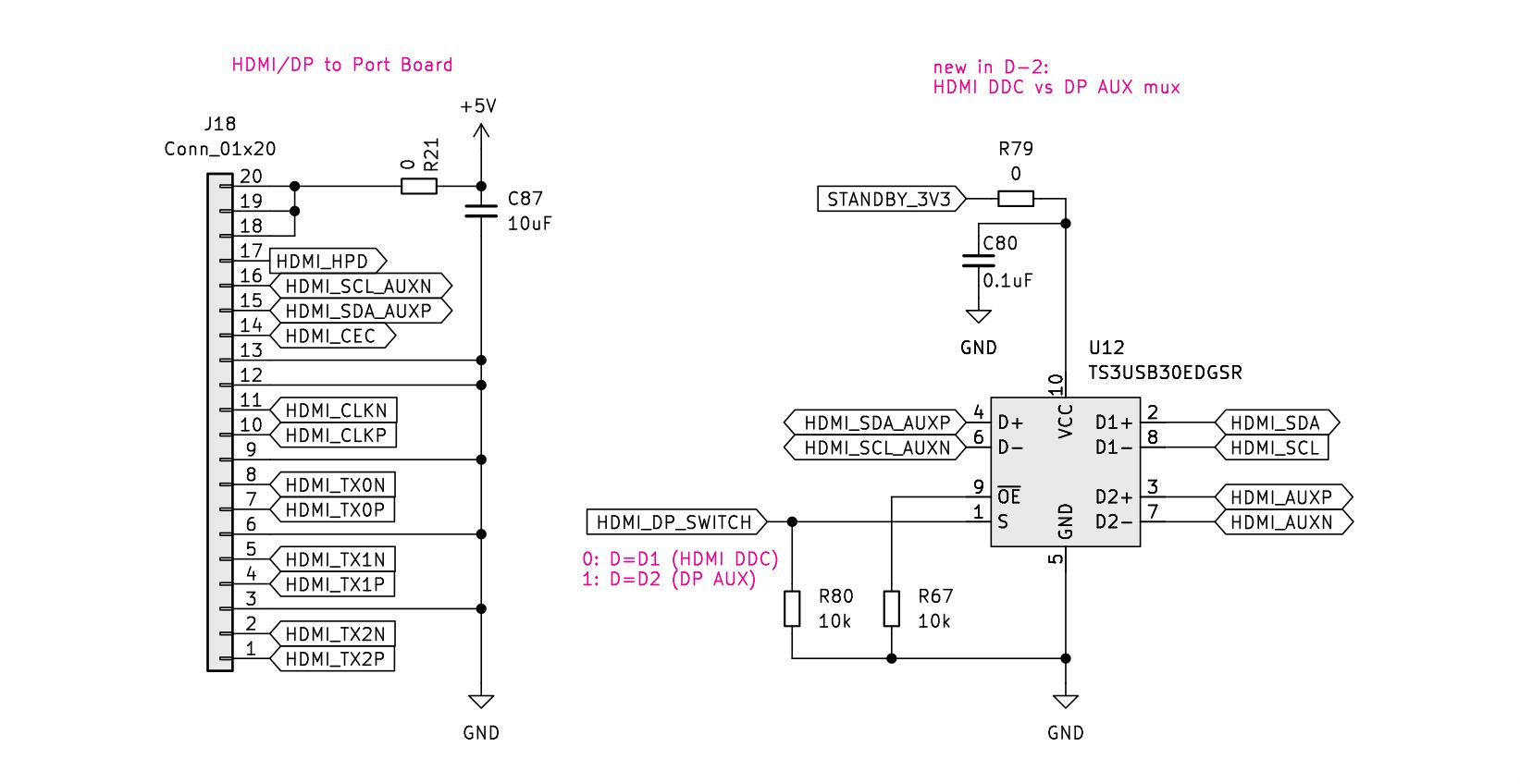
The latest iteration of the motherboard is designed so that one internal HDMI connector can carry DisplayPort signals instead, with HDMI’s usual I2C Display Data Channel pins muxed with an AUX lane for DisplayPort. So instead of HDMI going to the right Port Board, we could add in a theoretical future expansion—route DisplayPort signals to the left Port Board and mux it onto the USB PD connector, negotiating an Alternate Mode for DisplayPort using vendor messages on the PD data bus. But as USB Type-C alternate modes are notoriously tricky to get right, we’ll ship with tried and trusted HDMI at first. RK3588’s HDMI supports high resolutions and refresh rates. My personal sweet spot in my setup at home is a 27" 1440 p 120 Hz display from Dell (the U2724DE), which can charge the device and provide a USB hub with external keyboard, mouse and audio interface, as well as 2.5 GbE over a single USB Type-C cable.
Camera Acquisition
We had a lot of internal discussions, also in public on the Fediverse, about the inclusion of a camera in MNT Reform Next. The MNT Reform series traditionally has no built-in recording devices, but a camera can be very useful for video calls, scanning QR codes, or taking a selfie. NLnet, who funded a substantial part of our prototype development, also pushed for the internal camera feature for educational contexts.
Thanks to our modular architecture, we can fulfill both of these contradicting promises. I developed the electronics of our OSHW standalone USB camera into a new DIY kit version that can be optionally installed inside of the MNT Reform Next—but you don’t have to.
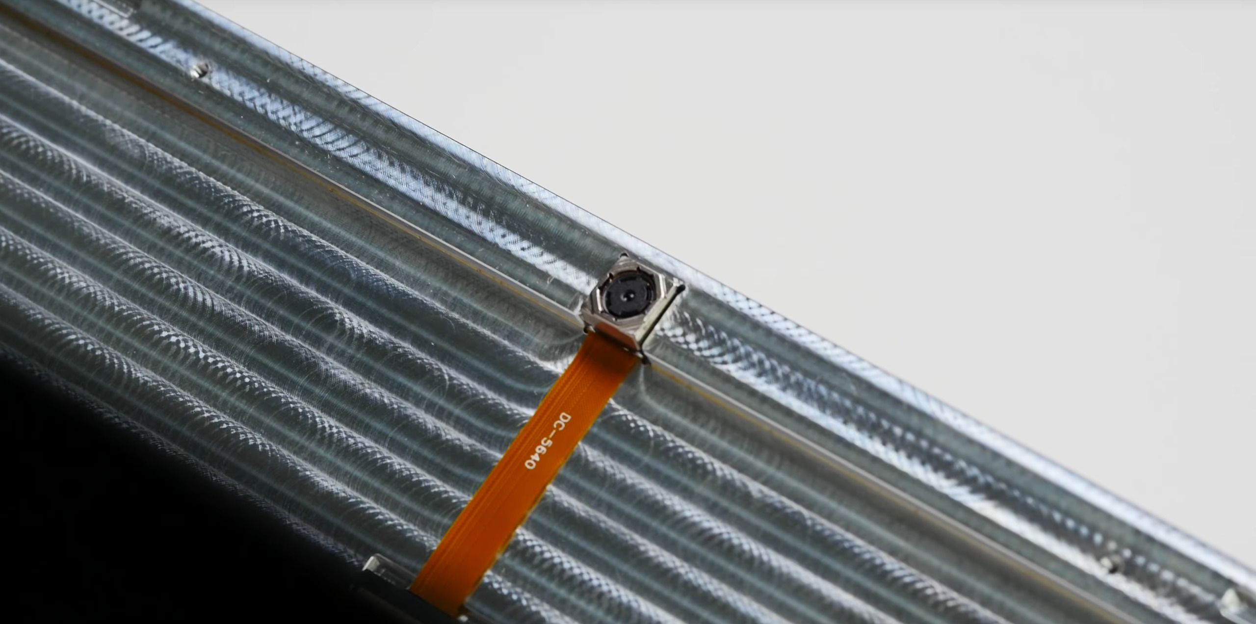
The sensor with autofocus lens is installed in a cavity in the screen back case above the display. The screen front part has a 2 mm hole that the camera can look through. Below the display sits an adapter PCB that converts the flat/flex cable of the image sensor for a JST-SH based cable that transmits the MIPI-CSI signal through the right hinge of the laptop. A camera acquisition PCB that is part of the camera kit can be installed on the 4x4 cm mounting grid below the keyboard. The Cypress CX3 chip converts the camera video signal into standard USB 3 or 2 UVC for use by the main processor. This module also has a connector for a hard powerdown switch and a LED that shows if it is powered.
WiFi/BT
With past Reform series processor modules like the NXP i.MX8MPlus and Amlogic A311D (Banana Pi CM4), we were married to certain Wi-Fi/BT chipsets that the module designers had chosen. This was not always optimal, as Wi-Fi driver quality, stability and firmware issues greatly vary on Linux.
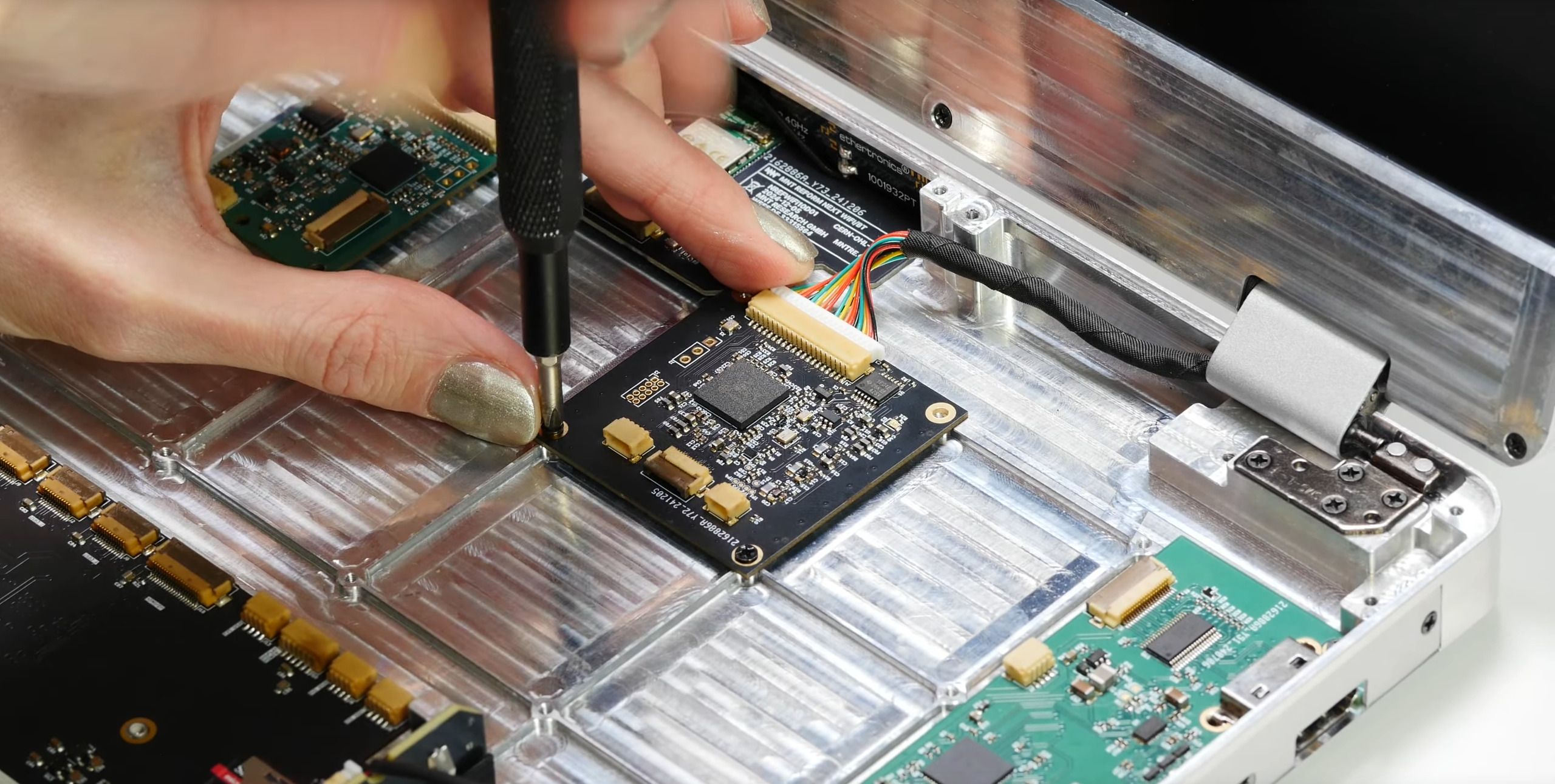
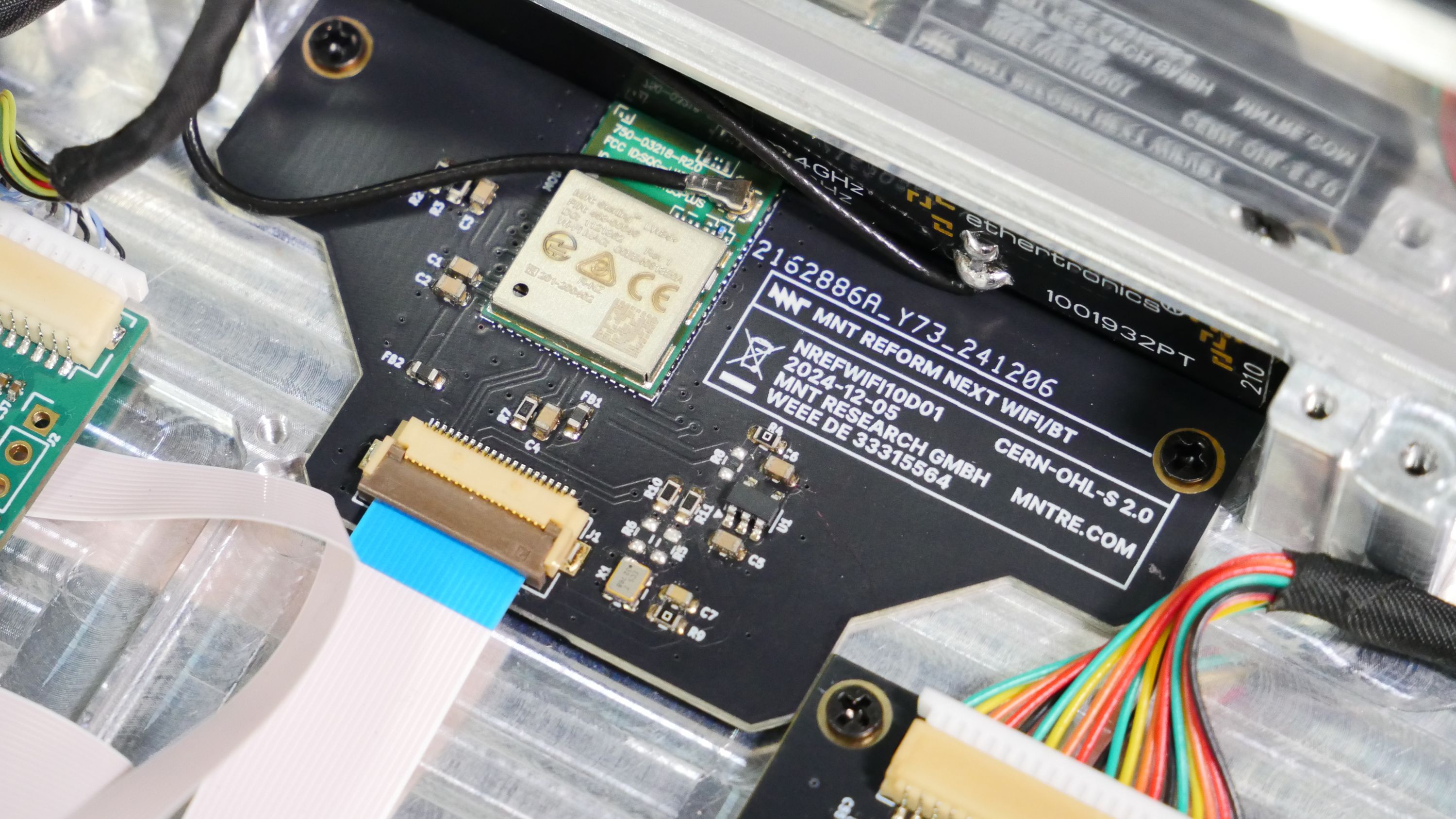
With the RCORE RK3588 module based around the Firefly iCore, we don’t have an integrated radio chipset. Instead, we can use any SDIO, UART or USB based chipset and put it on a PCB at the back of the laptop. To support this, I designed a new flex connector into the RCORE module that integrates the previously mentioned signals plus power. For our first radio module I chose the Ezurio (formerly Laird) Sterling-LWB5+ chipset that is based on Infineon CYW4373E silicon. It has a lot of flexiblity and can be driven over either USB or SDIO/UART. We also have an existing relationship with Ezurio as they bought Boundary Devices, who designed the i.MX8MQ and i.MX8MPlus system-on-modules that we used in previous MNT Reform systems.
PCIe and MicroSD Express
RK3588 is the first processor we’re shipping that has 4x PCIe Gen 3 lanes on one port (on previous chips, the max was 1x). For this purpose, I designated a group of unused/reserved pins on our 200-pin processor module interface for these new lanes. To stay inside the constraints of the Reform Next’s very small motherboard size, I chose the 2242 form factor for NVMe SSD disks and routed the 4 lanes to it. In quick read tests I got ~2.7-2.8 GB/sec. The choice of 2242 may be controversial for some as most disks on the market max out at 2 TB capacity, but I’m betting that it’s only a matter of time until 4 TB 2242s will be more widely available.
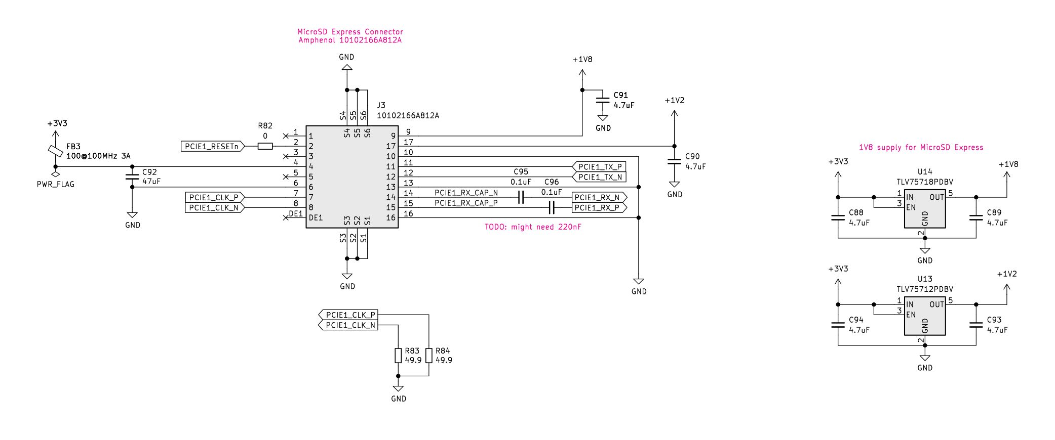
Last but not least, there’s a second PCIe controller (Gen 2 x1 on RK3588) and in the design phase I was torn for a while about what to do with it, as we didn’t have space for another M.2 card. The most immediately useful and compact interface I found was MicroSD Express. These futuristic little cards look almost exactly like MicroSDs and are backward compatible to them, but internally they are really tiny NVMe SSDs and can work at much faster speeds than traditional MicroSD cards. To make this possible, MicroSD Express has a secondary row of pins with a PCIe interface. And that’s what I connected on the motherboard of the MNT Reform Next, so you can easily add even more NVMe storage. You could also use it as your primary storage and break out the x4 M.2 connector to something like Oculink and drive an external GPU—there are endless possibilities for experimentation.
Until Next Time
I want to use this opportunity for a personal heartfelt thank you for supporting our campaign! We’ll have more to share in the next update.