Project update 6 of 13
Community Progress on Chip-on-Board Packaging Strategy
by Andrew WToday we have a guest post from Andrew Wingate (of Evezor Inc), sharing his perspective on the progress the wafer.space community has been making in developing a chip-on-board packaging strategy. This work includes contributions from Tiny Tapeout, MosBius (Columbia University), and community members like @Tholin and @xianglin_pu.
wafer.space exists to make custom silicon affordable. At $7 per chip for production quantities, the cost barrier to fabrication has been removed, but that’s only part of the story. Working with bare dies is challenging and typically requires specialized, expensive equipment.
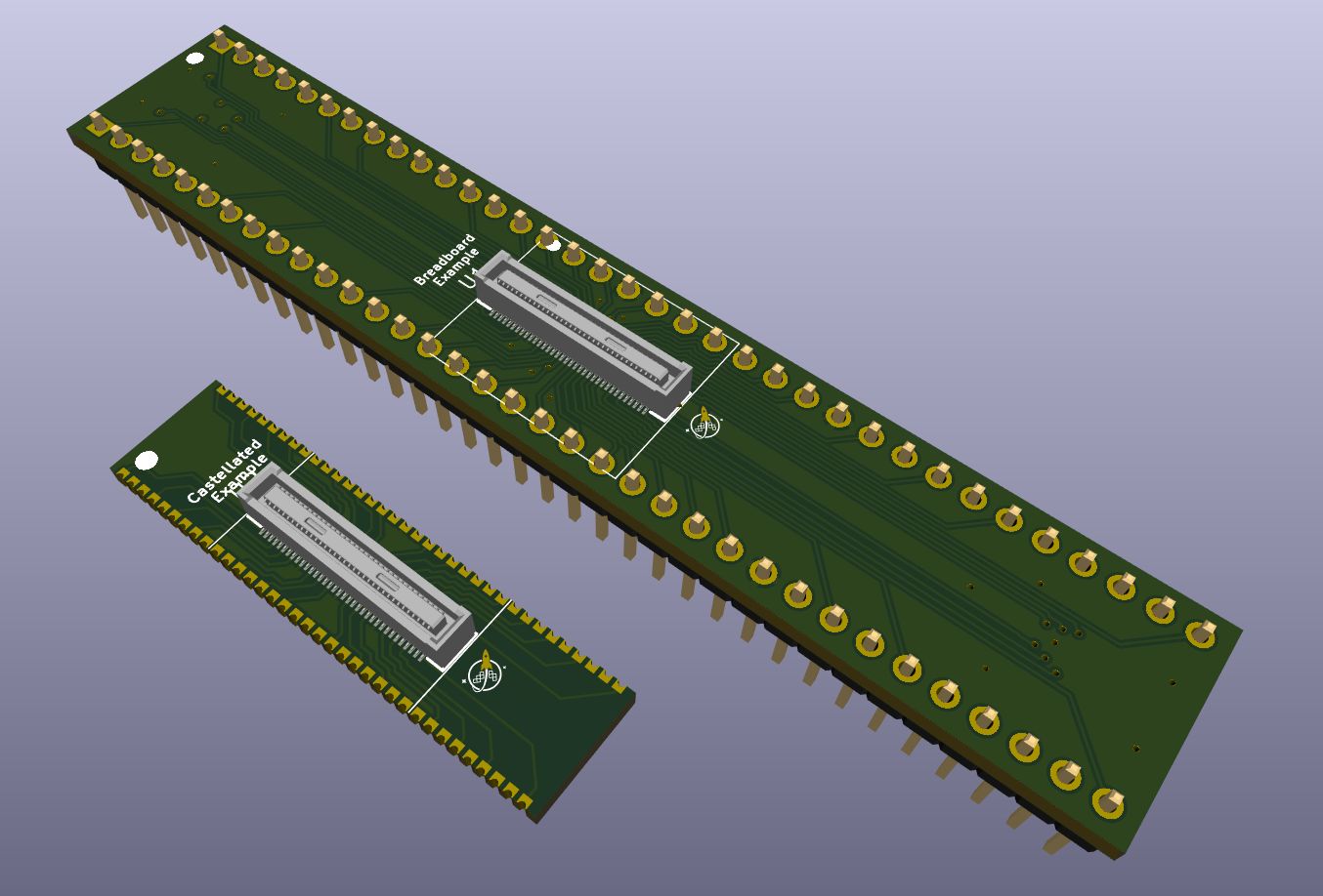
To make post-fabrication development more accessible, the community has been working on COB (Chip on Board) standard templates. Over the past months, various package options have been explored, including DIP, LGA, castellated breakouts, and breadboardable versions.
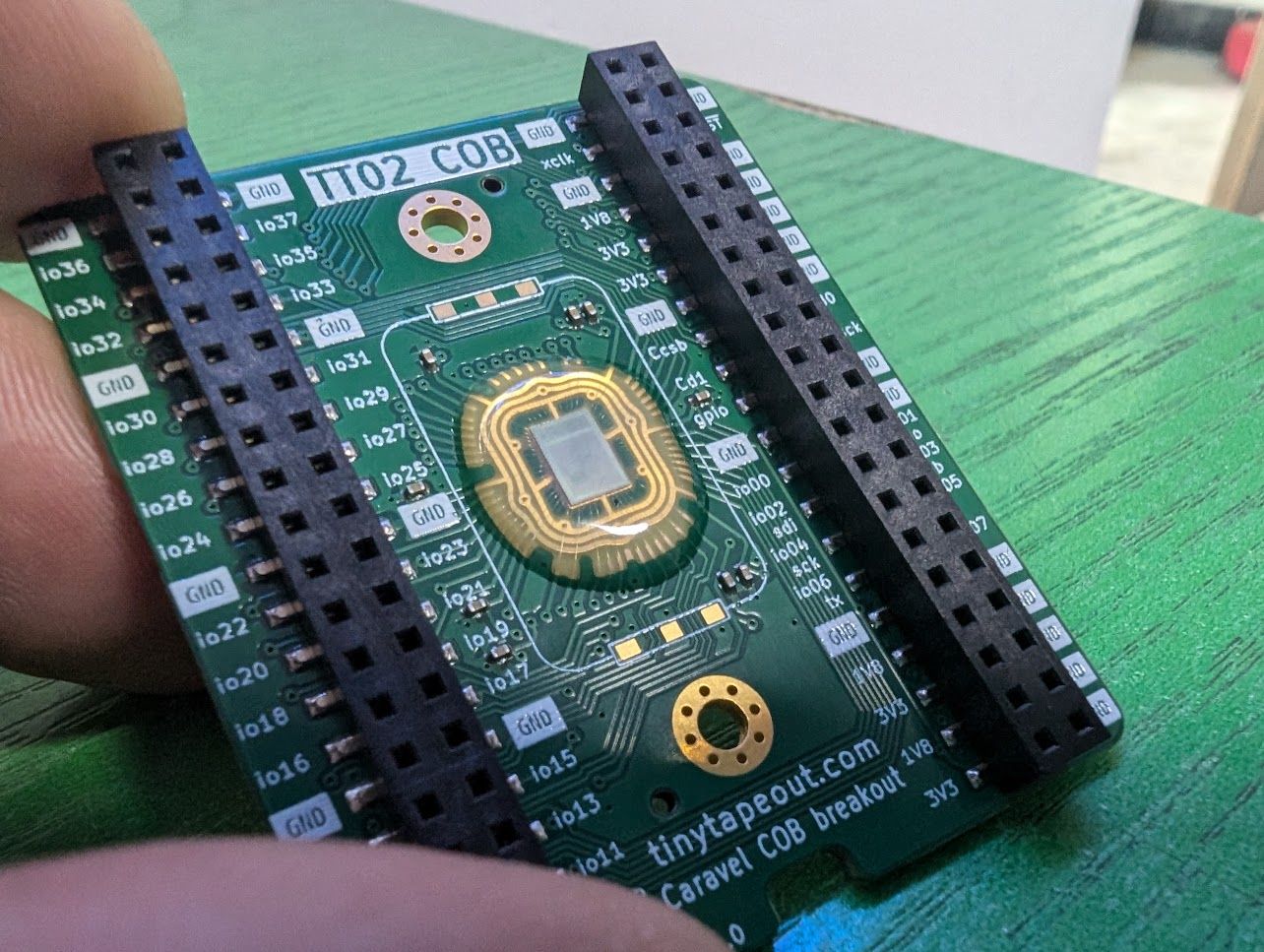
The leading contender is currently a mezzanine breakout board using connectors similar to those found on the Raspberry Pi Compute Modules. This design allows wirebonding houses to mount and wirebond your dies directly onto the COB packages, which can then be shipped to you ready for integration into your own systems.
When designing your motherboards, you’ll be able to source compatible connectors like this one and have your PCBA house assemble them. The community is also working on a range of breakout boards that follow a community-developed standard digital padring, to make development faster and more consistent.
What This Means For You: If you’re backing this campaign or considering it, you won’t need specialized equipment or expensive packaging services to use your chips. While the community continues developing these COB standards, wafer.space is offering wire-bonded COB packaging at buy.wafer.space for this campaign run (1,000 dies mounted and wire-bonded to PCBs). Alternatively, you can work with your own wirebonding partner using these community-developed designs. Either way, you’ll solder the connector to your custom PCB and plug them in just like adding any other component to your board.
The Community-Developed Standard Padframe and COB Design
While you’re free to use any pad configuration you wish, adhering to the community-developed standard ensures compatibility with wirebonding partners and simplifies the fabrication process.
Key Details:
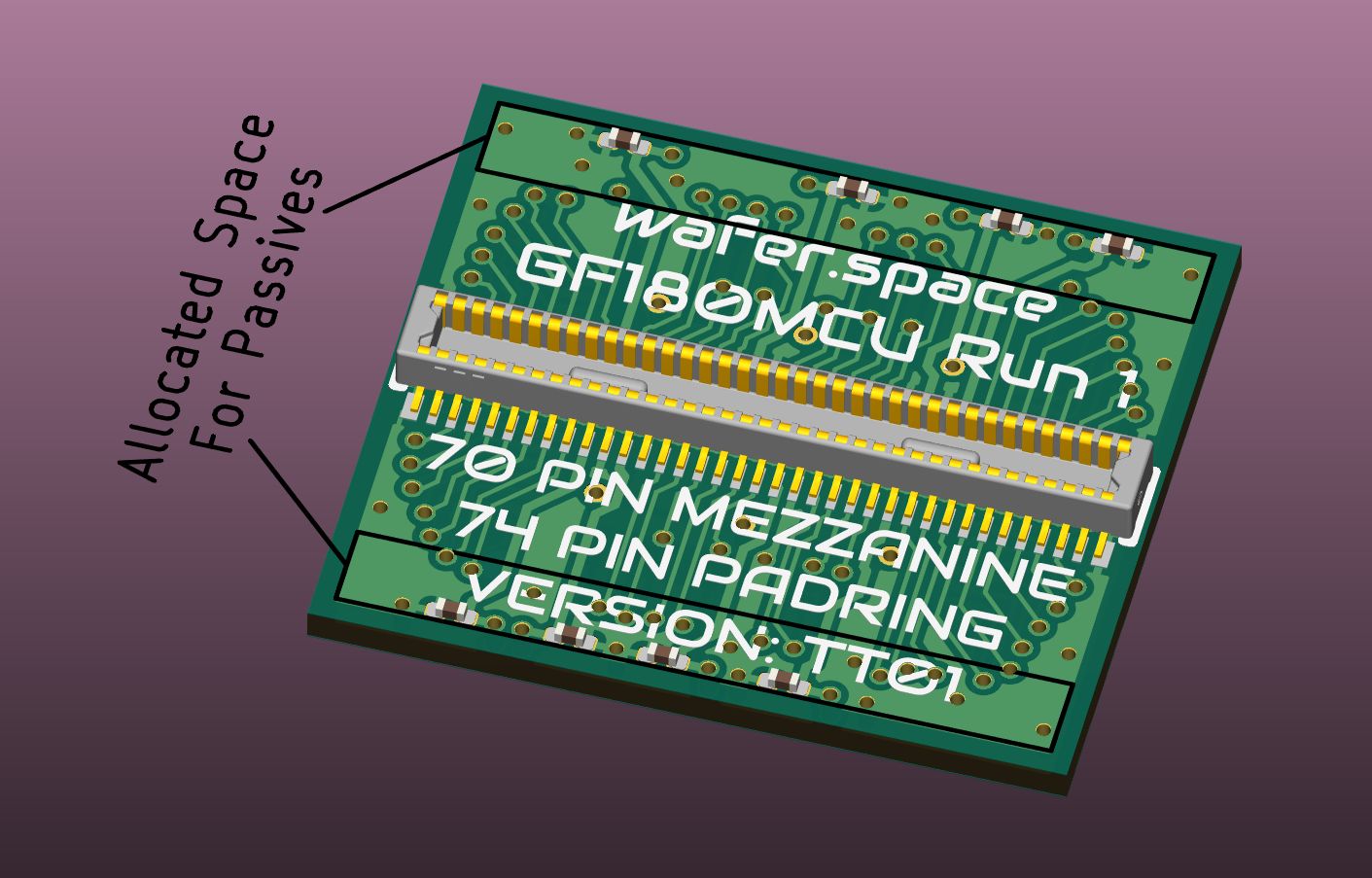
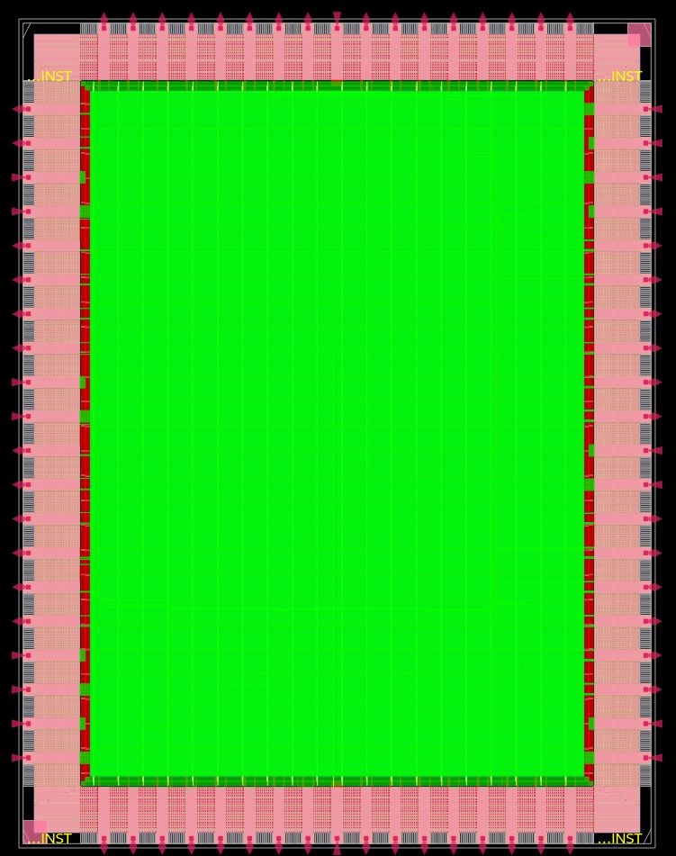
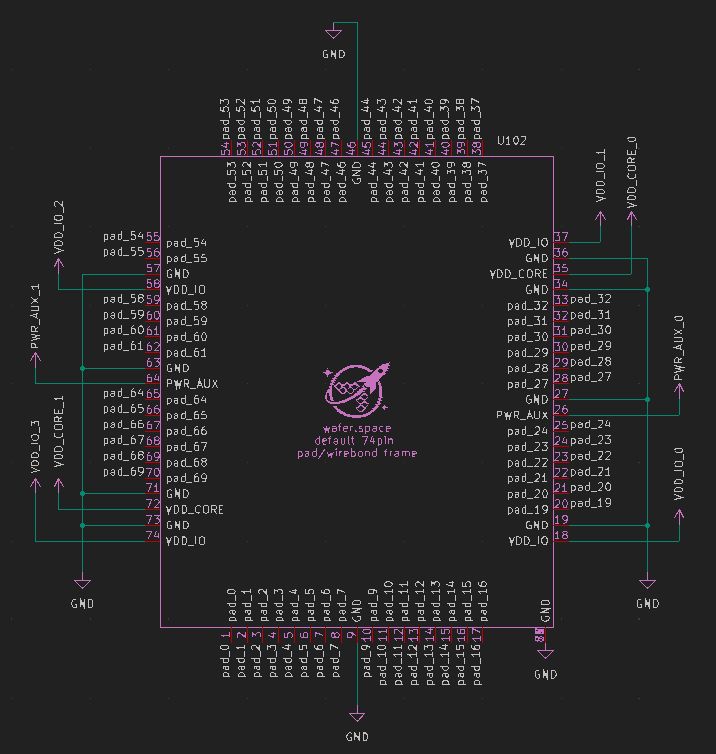
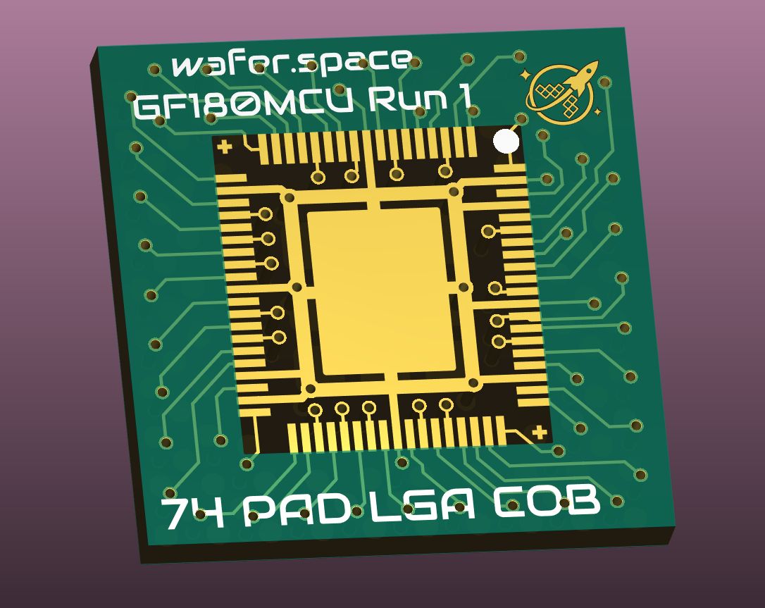
74-pad padframe on your die
20 pads on the east and west sides
17 pads on the north and south sides
74-pad wirebonding footprint
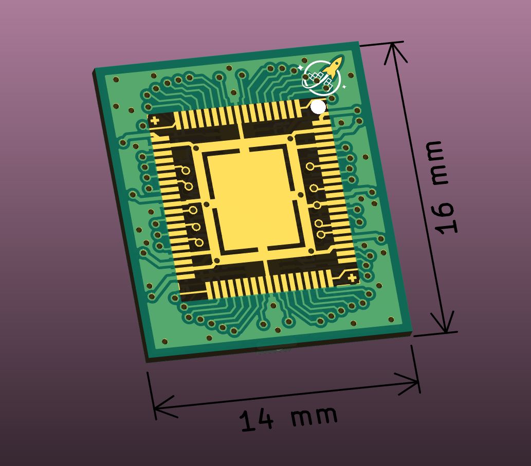
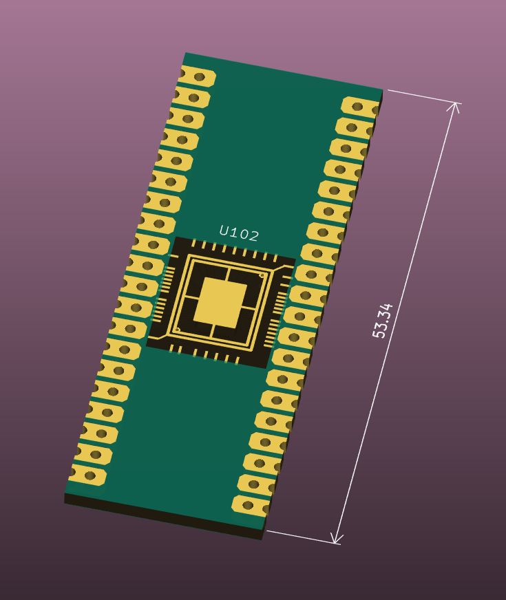
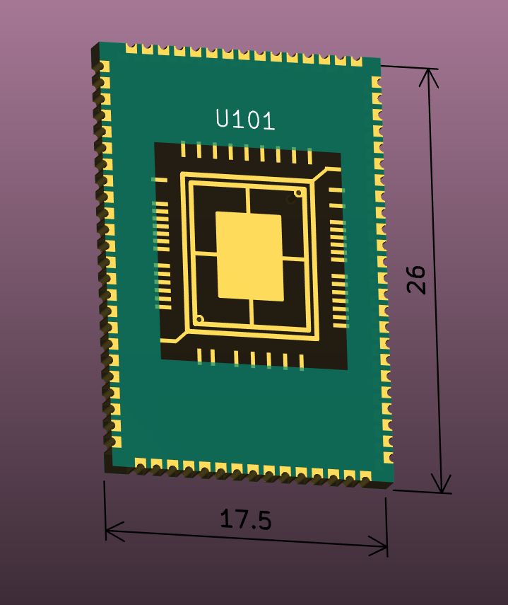
14 mm × 16 mm PCB
70-pin mezzanine connector: C19089236 or compatible
1 µF decoupling capacitors on VDD_IO, VDD_CORE, and PWR_AUX pins
Find most current designs on the chip-on-board-wire-bonded-pcbs repo
Why Standardize?
With the technical details established, it’s worth stepping back to consider why standardization matters for the open silicon ecosystem.
A Standard for the Broader Community
While this standard emerged from the wafer.space community’s needs, the goal is to create something that could benefit the broader open silicon ecosystem. By documenting the design openly and making the KiCad symbols, PCB layouts, and specifications freely available, other projects and communities could adopt or adapt this approach for their own chip-on-board needs.
The work you see here comes from contributors across the community: Discord members testing designs and providing feedback, Tiny Tapeout contributors sharing lessons from their COB runs, Columbia University students developing educational chips through the MosBius project, and veteran engineers refining the wirebonding footprints. Each brought different expertise: some from PCB design, others from silicon layout, still others from manufacturing and assembly experience.
The hope is that as more projects use compatible footprints and connectors, the ecosystem benefits grow:
- Wirebonding houses can optimize their processes for a common standard
- More off-the-shelf breakout boards and adapters become available
- Designers can share compatible motherboard designs across projects
- The barrier to entry for COB assembly continues to decrease
This isn’t about mandating a single approach. Diversity in packaging solutions remains valuable. Rather, it’s about establishing a well-documented baseline that communities can rally around when standardization helps everyone. If this standard proves useful beyond wafer.space, that would represent exactly the kind of collaborative progress that makes open silicon compelling.
This design hopefully meets the needs of a majority of projects on wafer.space. If your project needs something different, other open source packaging options are available to explore, such as the University of Washington’s BaseJump project, which offers BGA packaging standards including their 352-pin BaseJump Socket for designs requiring hundreds of I/O pins or more complex integration.
The Implementation: From Concept to Physical Boards
So what does this standard look like in practice? Let’s walk through the actual hardware, tools, and resources the community has developed.
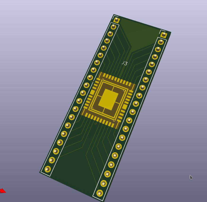
70-Pin Mezzanine COB
The centerpiece of the standard is a 70-pin mezzanine COB board that connects your wirebonded die to a standard connector.
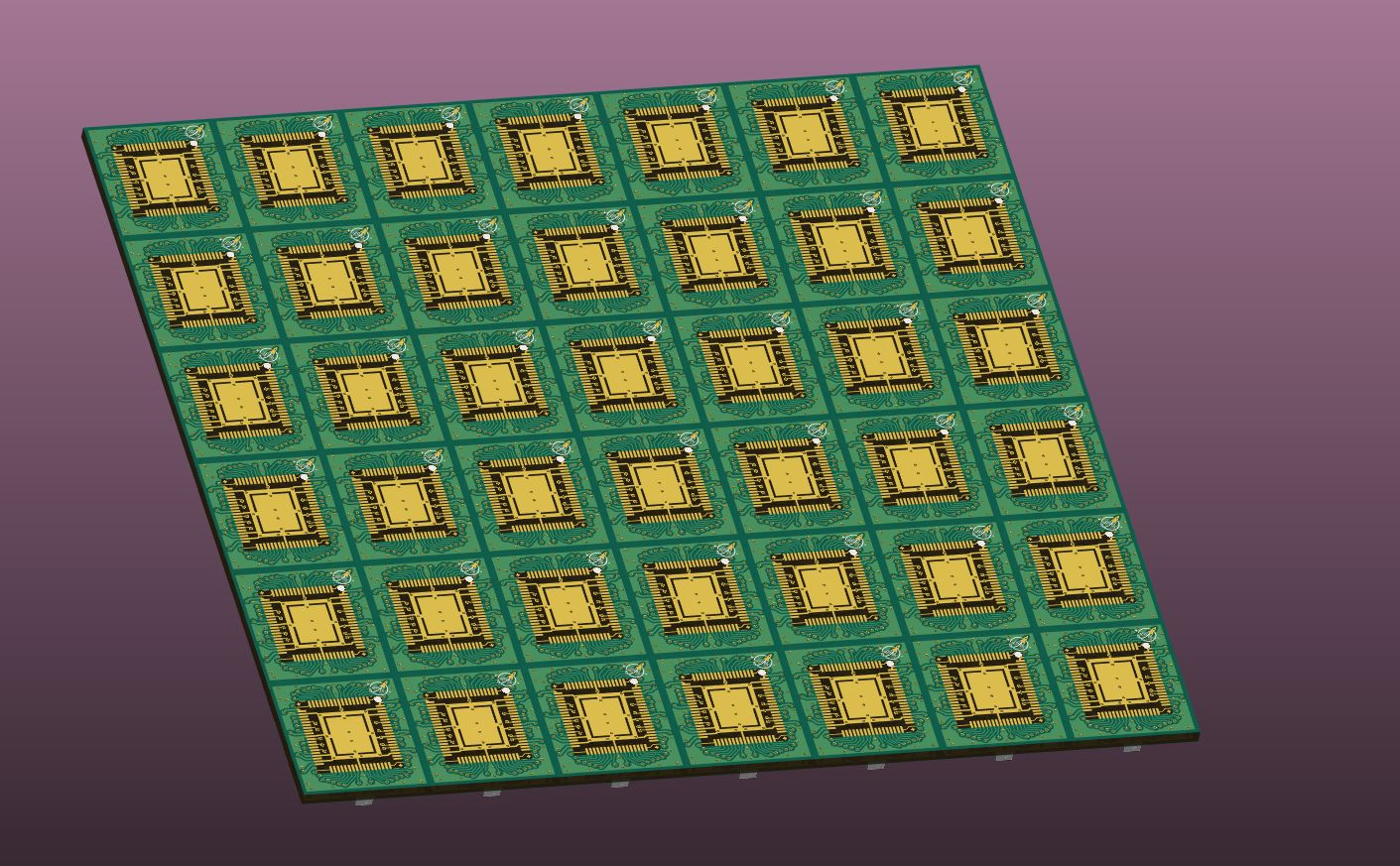
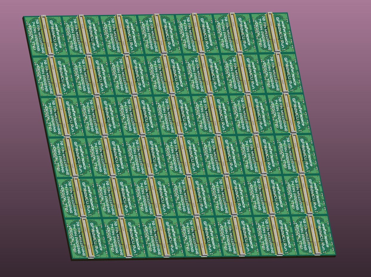
Panelized for efficient handling and assembly by wirebonding partners:
The standard configuration can be found in the GitHub repository. For easier viewing, it’s also available as a Google Sheet that shows the complete pad mapping.
To help visualize your own pad layouts, Discord user @Tholin has developed a Python-based pad viewer that generates an image of the pad layout defined in your template. This is useful for verifying your configuration matches your design intent. You can find the tool here.
Design Tools and Ecosystem
Having the physical COB boards is only part of the picture. To actually use them, designers need schematic symbols, footprints, and integration tools. Here’s what the community has built to support the full design workflow.
Default KiCad Symbols
The community has developed several KiCad symbols to support design and integration with COB layouts.
The pad mapping symbol corresponds to the default 74-pad wirebonding padframe and default configuration from the GF180MCU Project Template.
Some users have suggested reducing the number of ground and power pads. If there is sufficient demand, an alternate default configuration will be created.
Join the discussion on our Discord server.
70-Pin Mezzanine Connector Symbol
The mezzanine connector symbol provides a 1:1 pin mapping to the 70-pin default layout.
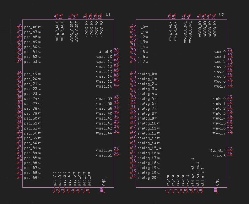
All pins are aliased to match Tiny Tapeout naming conventions, useful for those familiar with the TT ecosystem who are designing custom chips for this wafer.space run.
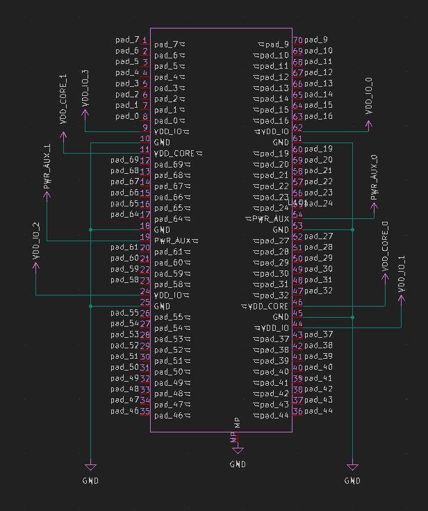
An alternate version is also available that organizes pins by signal type. This version is particularly useful for Tiny Tapeout-style breakout motherboard designs where grouping by function makes routing clearer.
KiCad Resources for COB Design
While the initial symbols are in KiCad, the community welcomes contributions of symbols and libraries for other PCB design tools. If you use Altium, Eagle, or another tool, please submit a pull request to the chip-on-board-wire-bonded-pcbs repo!
For those new to KiCad or looking to deepen their PCB design skills, Pat Deegan (developer of the Tiny Tapeout demo board) offers KiCad:Unlocked, a comprehensive free course that covers everything from basic circuit design to advanced PCB layout techniques. The community hopes to work with Pat in the future on a tutorial specifically focused on wire bonding integration and designing motherboards for wafer.space COB packages.
If you want to quickly review KiCad designs without installing software, KiCanvas provides a browser-based viewer for KiCad files. You can use it to inspect the standard COB layouts, verify connector pinouts, and review community-contributed designs, all directly in your browser.
Beyond the Standard: Expanding Options
While the 70-pin mezzanine connector serves as the standard, the community recognizes that different projects have different needs.
Castellated and Breadboardable Breakouts
The community is developing a series of breakout boards designed to make it easier to prototype, experiment, and integrate your dies into existing systems.
Real-World Adoption
The real test of any standard is whether people actually use it. Here’s how the community is already building on this work.
Derivative Designs
It’s exciting to see others building on the wafer.space platform!
Professor Peter Kinget and his students at Columbia University are developing educational chips using wafer.space for their MosBius Project.
MosBius provides students and designers the opportunity to explore MOS circuit topologies through a unique analog switch matrix, where each pin can connect to any of ten on-chip buses. This enables flexible on-chip circuit wiring and simplifies testing setups.
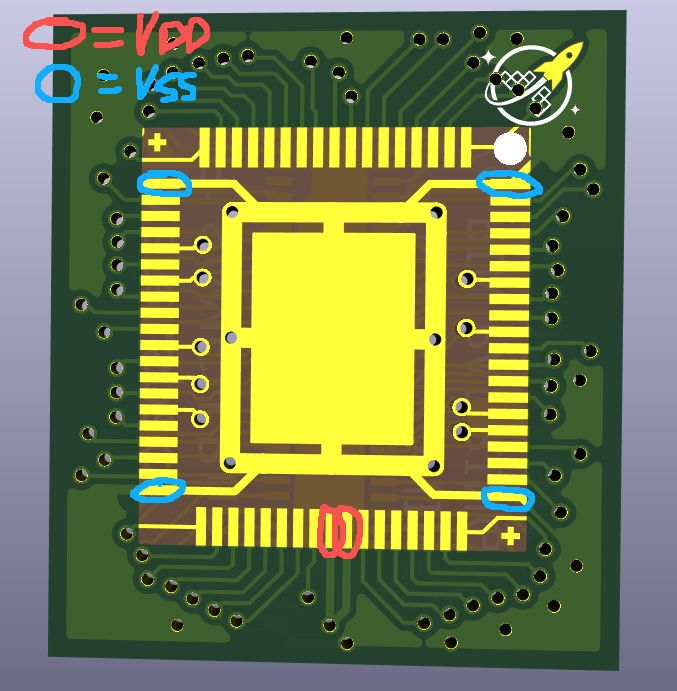
Image and design by @xianglin_pu on wafer.space Discord
The Path Not (Yet) Taken
Before settling on the mezzanine connector as the standard, the community explored several alternative packaging approaches. While these didn’t become the primary standard, they represent valuable experiments that informed the final design and may still serve specialized use cases.
LGA (Land Grid Array)
DIP
Castellated
Learning from Pioneers
The wafer.space COB work doesn’t exist in isolation. Other projects have tackled similar challenges, and their experiences directly inform this effort.
Tiny Tapeout recently published an update on their first successful Chip-on-Board (COB) implementation, highlighting their bare-die submission on the Zero to ASIC Course "MPW-7" run.
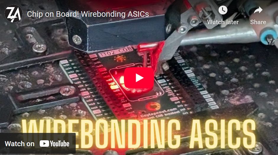
Watch the video: Tiny Tapeout 9 - First COB samples!
While Tiny Tapeout achieved a significant milestone, they also noted limitations: the long bonding wires increased inductance and degraded performance, and securing small-volume wire-bonding services remains difficult.
For those interested in understanding the wire bonding process in detail, Stephan Bökelmann’s talk at Kicon 2025 provides an excellent introduction to the practical challenges and techniques:
Watch: Poor man’s intro to Wire-Bonding @ Kicon 2025
The wafer.space community views these learnings as a springboard. By introducing standardized COB templates, the goal is to make COB packaging more accessible, more scalable, and better optimized. The objective is to build upon the success of Tiny Tapeout and improve their future runs by reducing parasitics, streamlining the supply chain, and enabling anyone to pick up a COB-mounted die and integrate it into their system with ease.
Join the Effort
This community-developed standard is exactly that: community-developed. The designs, symbols, and approaches documented here represent months of collaborative work, but they’re far from finished.
The community is exploring multiple COB packaging varieties and would love your contribution:
If you’re designing a chip for this run:
- Share your I/O requirements in the #cob Discord channel. Your needs help refine future designs
- Test the pad viewer tool and report any issues or feature requests
If you have COB or wirebonding experience:
- Share vendor recommendations or tips for small-volume runs
- Provide feedback on the wirebonding footprint design
- Help identify potential manufacturing issues before they become problems
If you use other PCB design tools:
- Contribute symbols and footprints for Altium, Eagle, or other platforms
- Submit pull requests to the chip-on-board-wire-bonded-pcbs repo
If you’re curious or have questions:
- Ask in Discord. The community includes experienced designers happy to help
- Review the designs using KiCanvas and suggest improvements
- Help test breakout board designs and report what works (or doesn't)
Join the community and help shape the future of accessible silicon design:
Discord: discord.gg/43y2t53jpE (see #cob channel)
Matrix: #gf180mcu.org
Together, the community can make custom silicon as easy and affordable as PCB design.
Thanks to Andrew Wingate for this guest post! If you’re interested in chip-on-board packaging, join the #cob channel on the wafer.space Discord to discuss designs, share feedback, and help contribute to making COB packaging accessible for everyone.