Project update 3 of 13
Production Progress and Some History
by Andy HaasHello Haasoscope Pro enthusiasts,
The campaign has been live for two weeks now and we’re already almost halfway to our funding goal, with four weeks still to go! Thanks to all of you who have supported the project already.
Production Update
The board and hardware design is officially production ready at this point, after testing a very successful final beta revision this past week. It has a refined anti-alias filter, a bug fix to the (optional) external 12 V power input selection (that no longer conflicts with USB-C power detection on MacBooks), and better looking LEDs (now on the main board, with light pipes going to the front panel).
We’re hard at work on some software improvements too, like the addition of eye diagrams for high-speed serial debugging, better saving of events to disk, more intuitive layout of menus and controls, etc. Also, the community is getting more involved. Dmitri P. has a beta unit now and is working on adding Haasoscope Pro support for his universal Python scope API, which will make it really easy to interact with the device from your own scripts! More on that in a future update. If you are interested in contributing to the Haasoscope Pro project, get in touch with me! I still have a few more beta units available.
I want to spend the rest of this first full update telling you some of the history of developing the Haasoscope Pro, and what pieces had to come together to make it possible.
History of Haasoscope Pro
As I advanced in the kinds of electronics projects I worked on, such as one of the world’s fastest random number generators, I found myself needing a much faster scope, in the 1-2 GHz range. But I was shocked at how expensive they are, around $10,000 (USD)! Even the required active probes were over $1000 each! I started low-key investigating why this stuff was so pricey, looking at available ADCs, and thinking about possible designs.
I was inspired earlier in 2024 by an open-source 2 GHz active scope probe on hackaday. I printed and assembled a few of my own, and they worked great, for only ~$100 each! The probe was already half the challenge - now I just needed a fast, affordable USB scope.
The main challenge was the huge data rate needed. A 12-bit ADC running at 3.2 GS/s generates ~50 Gb/s of data (including all the clock and strobe and sync signals along with the samples). That all needs to go from the ADC to an FPGA, where it is processed. There are two standard ways of transmitting data this fast into an FPGA. The "fancy" way is high speed serial links. These can run at ~10 Gb/s each or even higher, so with just ~4 or so you could handle it. BUT, FPGAs with high speed serial links are a) more expensive b) usually require the paid firmware development software licence and paid IP for commercial products and c) those 10 Gb/s differential traces are very tricky to route properly (especially on standard FR4) since very high frequencies are involved.
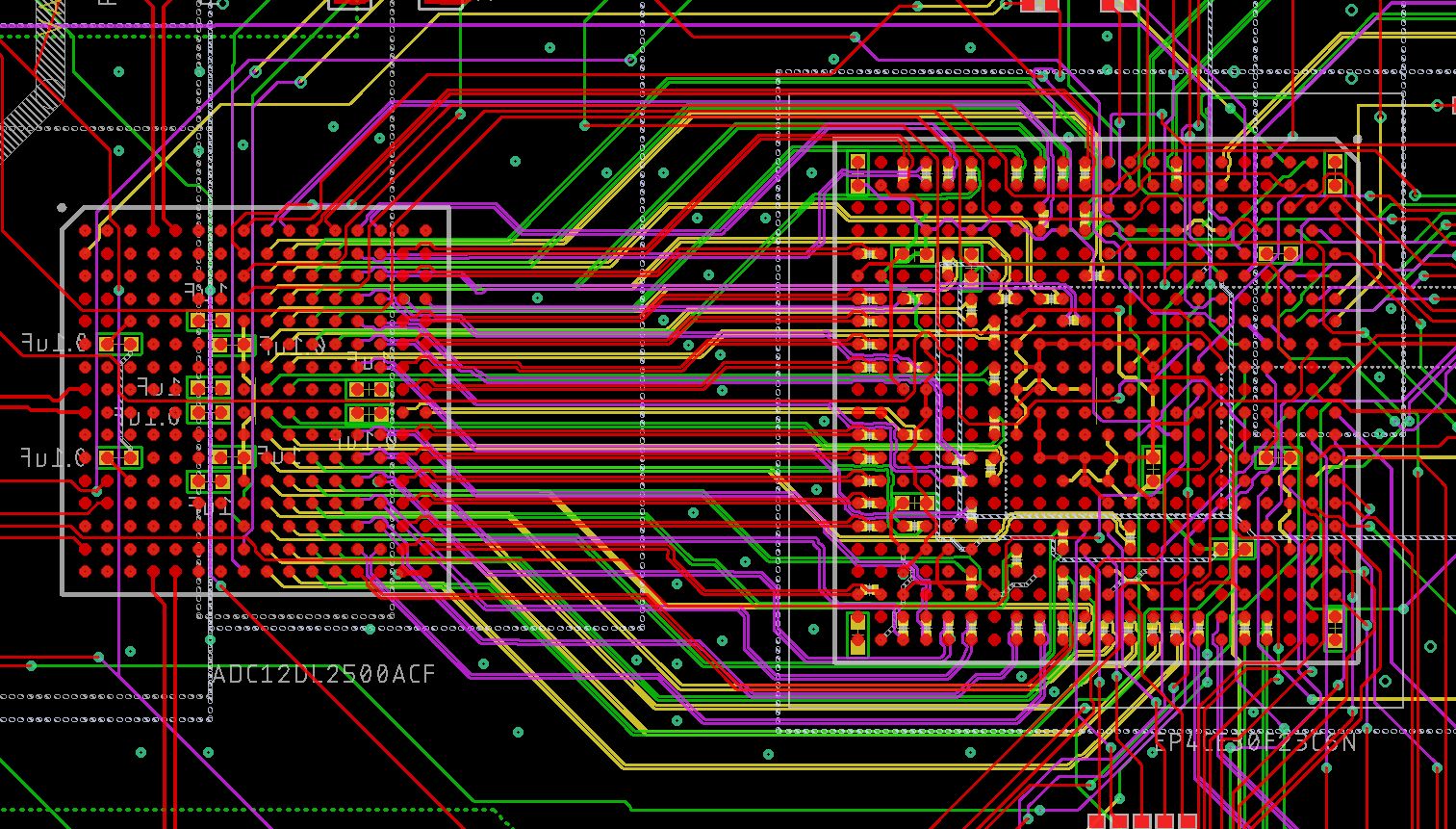
But there’s also an older method: LVDS. Those links run at just ~1 Gb/s each, but FPGAs often have more than 100 of them available. They are easier to route since each is lower speed. And they’re supported by the free FPGA software versions with no licence or IP required. I eventually stumbled upon a high-speed ADC chip, strangely affordable, that had a parallel LVDS interface. I still had to deal with a 256 pin 0.8mm pitch BGA for ADC and a 484 pin 1 mm pitch BGA for the FPGA, and routing ~80 LVDS differential signal pairs, each running at 800+ Mb/s, but it finally sounded doable in principle.
I eventually managed to get the routing to work with "only" a ten-layer PCB and no blind or buried vias. I needed very thin 0.09 mm traces to fit pairs of them between BGA pads, and small 0.2 mm vias directly under the BGA pads, plus 56 0201-termination resistors on the bottom of the board under the FPGA. Turns out that all is at the limits of some of the standard PCB fabs, but some can do it. This is what the board layout looks like in that area, with the ADC on the left feeding the FPGA on the right. Different colors are different signal layers.
A very important lesson I’ve learned, the hard way, while doing other projects, is to break a large project into as many small blocks as possible. Don’t put everything on one board at first. Start with each block on its own little board. Then, it’s quick, easy, and cheap to test and iterate versions of each little board you’re working on, without redoing and even potentially messing up the other boards that already work fine.
I first made a board with just the FPGA on it, to get that working on its own. The board didn’t really do anything except prove I could power it, program over JTAG, see a 50 MHz clock input from the crystal, and make some LEDs blink. The board worked just fine, first try!
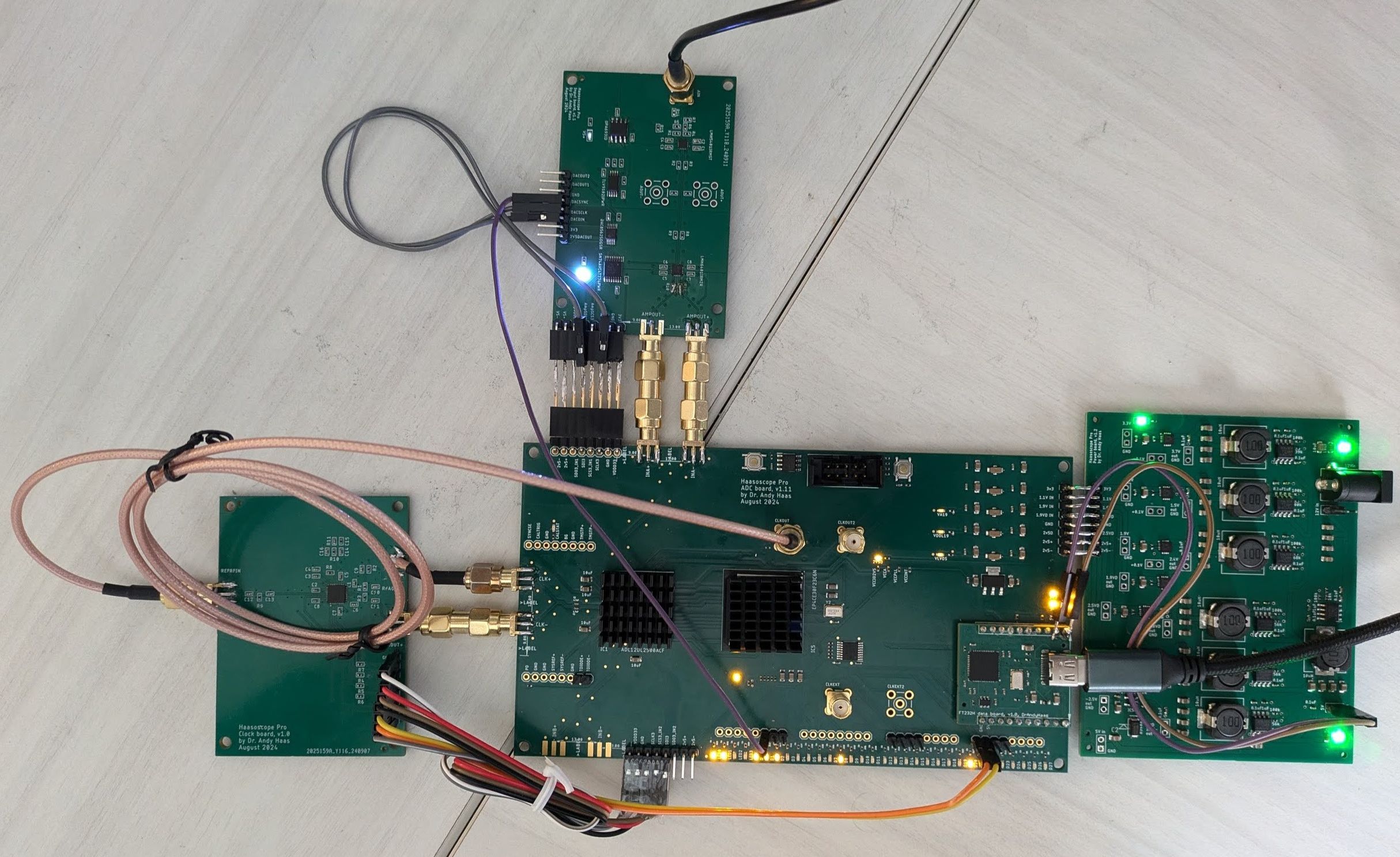
Then I was ready to make a board with an ADC and an FPGA on it. You can see below what the "ADC FPGA board" looked like, with all the other smaller boards hooked up to it. There’s a "power board" to provide the ADC and other things with all the voltages they need (on the right), an "input board" (on the top) to do the single-ended to differential conversion plus amplification of the analog inputs to the ADC, and a "data board" (attached to the USB cable) that talks over USB-2 to/from the FPGA. The high speed differential 1.6 GHz low jitter clock is supplied by the "clock board" (on the left), which I basically just copied from the ADF4350 datasheet.
The last board I worked on was the pre-input board that handles annoying analog stuff: 50/1M switching, AC/DC switching, attenuation, anti-alias filtering, etc. It mostly worked fine too, though I had to mess around with different relays, connectors, and photo mosfets to maintain the 2 GHz of bandwidth. I even had to buy a cheap but wonderful NanoVNA V2 PLUS4 vector network analyzer to debug it all. Maybe more on all that in another update.
All these individual test boards are still available in the GitHub repo in the "sub boards" directory.
The final step was just to combine all the test boards together onto one board and we had the first full prototype of the Haasoscope Pro!
If you’ve made it this far, thanks for your interest in the Haasoscope Pro oscilloscope and Pro-be active probe project. Please pledge your support today if you think this is a valuable open-hardware product, and you’ll soon have your very own GHz-class scope and/or probe on your bench!
