Project update 2 of 11
Exploring the Design Essence of WiSer
by Jaydeep DHello everyone,
I want to express my sincere gratitude for the overwhelming support WiSer has received in the first week of the campaign. Your enthusiasm has already propelled us past our funding goal, and it’s truly heartening.
As we navigate through this exciting campaign journey, I wanted to take a moment to share some captivating insights into the design aspects of WiSer; I believe you’ll find these details intriguing.
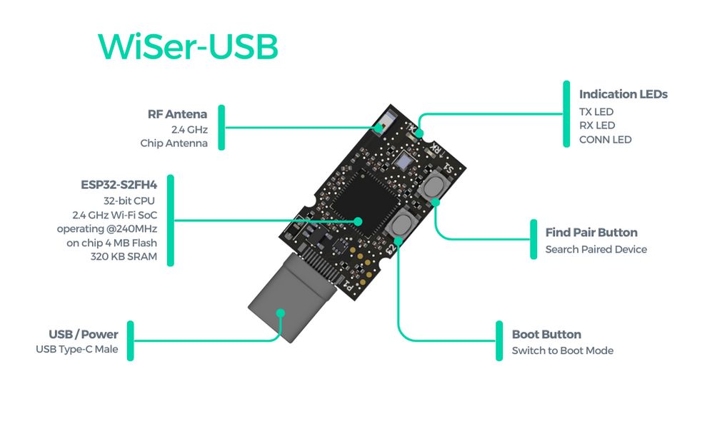
In the WiSer-USB design, the central component is the ESP32-S2 SoC, responsible for processing and wireless communication. Notice the two buttons: the "FIND PAIR" button is used to identify the paired device, and the "BOOT" button is used to load firmware onto the ESP32-S2. The TX and RX LEDs signify data communication in their respective directions. The RF chip antenna was chosen to keep the USB portion as small as possible. Power supply and data communication are through a USB-Type C male plug connector. The reason for choosing it over the typical USB-A connector is to have native compatibility with modern devices, given the increasing use of USB Type-C in recent years. Besides this, it also facilitates direct adoption on Android phones/tablets without any converters. Lastly, the half-circled notches you see on the three sides of the PCB serve a purpose—they hold the PCB in place inside the enclosure. This notch design was made based on the desire to have the PCB and enclosure fitted together without any screws. There is a lot to discuss about the design aspects of the enclosure as well, but maybe we’ll cover that in a separate update!
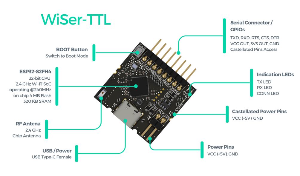
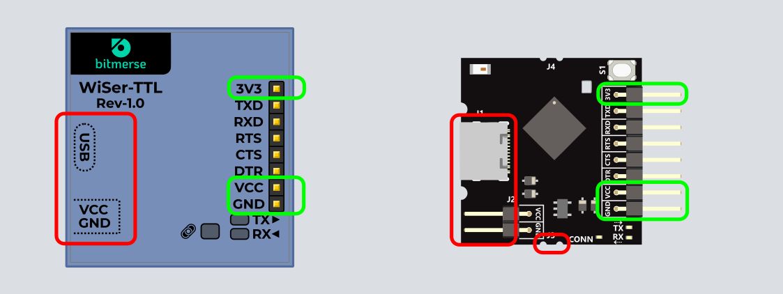
Now, let’s take a look at the WiSer-TTL design. The major components are the same, with a few additions/omissions considering TTL side requirements. For example, on the TTL side, there’s no need for a "FIND PAIR" button, as that functionality is handled on WiSer-USB, but we have a separate "CONN" LED to indicate connection to the paired WiSer-USB. Similarly, the power supply connector needs to be a receptacle instead of a plug, hence the USB Type-C female connector. Here also, we’ve used half-circled notches for enclosure fitment. On the TTL side, we have serial pins along with power output pins. Speaking of power, let’s dive into the design aspects of the power section. As shown below, connections marked in red are used for receiving power (a.k.a. power input), while connections marked in green are used for delivering power to the target device (a.k.a. power output).
One area we haven’t talked about much is mounting WiSer-TTL onto custom PCBs. WiSer-TTL is designed to be easily integrated with your custom PCB design. The castellated pins are used to solder the WiSer-TTL and custom PCB together. The WiSer-TTL can be placed in different possible locations, as shown below.
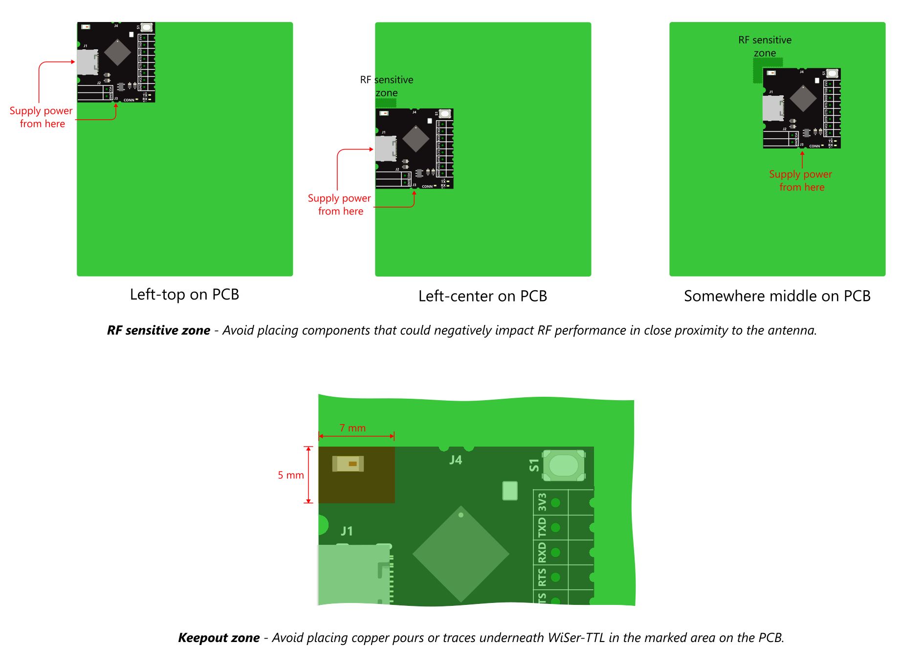
Power can be supplied using USB or header pin, and the power output pins can be used by the PCB to draw power. This way, a custom PCB can eliminate the USB connector and power circuitry altogether. Consider the reverse scenario, where power is already generated by the custom PCB, which can then be fed to the castellated pins on the bottom of WiSer-TTL. Interesting, right?
I hope these in-depth details excite you and we will strive to bring more such insights in upcoming updates!
Feel free to connect with us if you have any questions, ideas, or if you simply want to share your thoughts.
Thanks again for your support, and if you get a chance to spread the word about WiSer, we would be immensely grateful!