Project update 2 of 13
A tour of our schematics and PCB
by Andy WilsonHi everyone,
Many thanks to everyone who has been in touch so far to ask a question, back PICO DSP, or share the project! For our first update, let’s take a look at the schematics and see what’s happening on the PCB. The schematic is available in our GitHub repo.
Schematics Sheet 1 – Power and USB
Power is delivered to the board via two routes: (1) by the battery connector or the VIN pin, which are on the same net, or, (2) by USB. The maximum input voltage on VIN is 6 V, which is the maximum input voltage of the analog and digital regulators. The top regulator, with output VDD, supplies a regulated 3.3 V for the ESP32 and the digital sections of the WM8978 codec. The other regulator, output VCC, supplies a regulated 3.3 V for all the analog sections of the WM8978 codec, and the power for the MEMs microphones.
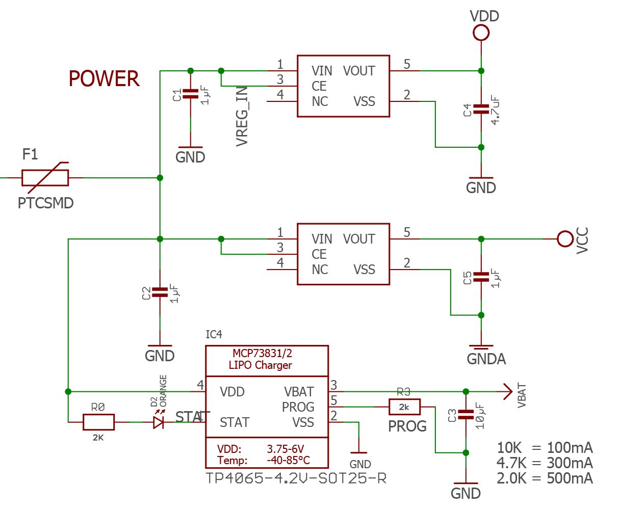
Q1 is a P-channel MOSFET in a power switching configuration. When there is voltage on VIN (e.g., 3.7 V) and USB is not connected, there is no difference between the gate and source, and maximum current flows from source to drain. The input voltage to the regulators will be the same voltage, 3.7V. When USB is connected, the 5V input voltage on VBUS is also applied to the gate of the MOSFET, restricting the current flow from source to drain. The input voltage to the regulators will be 5V minus the diode drop from D3, approximately 4.6V, and the current draw is shared between the two power sources. Diode D3 prevents current from VIN from flowing into VUSB when there is voltage on VIN, protecting USB ports upstream of the device. In this configuration, it is possible to power the board from a battery or external power supply and then safely plug and unplug the USB cable for programming, or power the board from either the USB port or VIN.
F1 is a resettable PTC fuse which provides over-current protection, rated at an iHOLD current of 750 mA, the maximum current that the PTC fuse can sustain for long periods of time, and an iTRIP current of 1.5 A, which is the minimum current required for the fuse to heat sufficiently to switch into a high-resistance state, limiting current flow.
The Lithium Polymer battery charger is MCP73831 and is configured to charge at 500 mA when it reaches constant current mode. The USB-to-serial converter used in this project is the CP2102N and is configured with the internal regulator bypassed. As recommended in the datasheet and investigated during prototyping, the voltage on the VBUS pin is dropped using a voltage divider to ensure reliable operation.
IC8 just below the CP2102N provides ESD protection for the USB data signals. The dual NPN transistor Q2 is a circuit that connects to the EN and IO0 pins of the ESP32 and, when used with the ESP32 bootloader code, allows for auto-programming and rebooting of the ESP32.
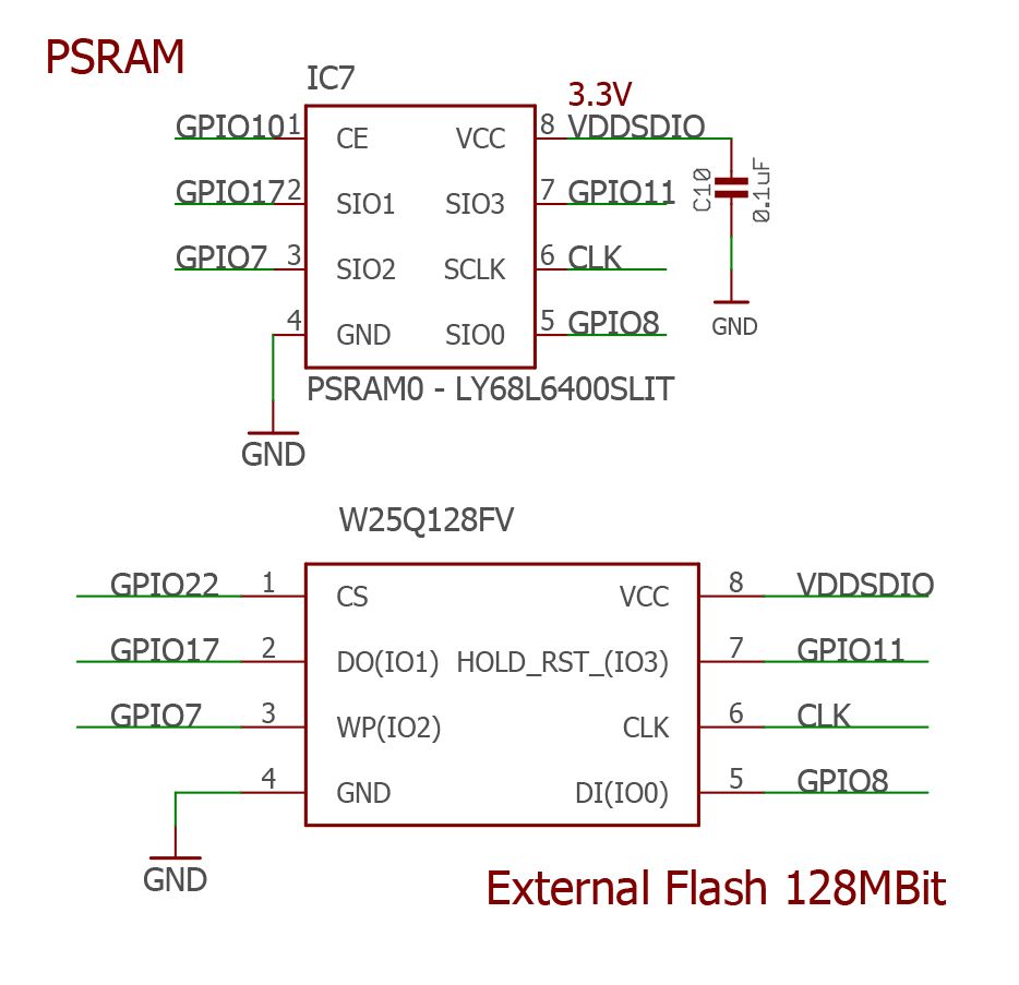
Schematics Sheet 2 – MCU
The MCU is a ESP32 Pico D4 and is implemented with external components following the recommendations in the datasheet and the Espressif hardware design guidelines. The antenna is connected on net LNA_IN, which is a 50 ohm matched impedance trace. The PCB stack up, the copper width of this trace, and the matched LCC impedance network of L1, C11, and C12 are calculated to match this value.
The PSRAM and 16 MB Flash are also included on this sheet, only one of these memory IC’s are populated on the PCB, note the different CS pin for the 16 MB Flash. On this board, the voltage for the Flash, VDDSDIO, is 3.3V. The green status LED is connected to IO5 and the button to IO36.
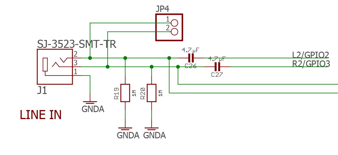
Schematics Sheet 3 – Audio
The audio codec, microphones, and line inputs and outputs are on sheet 3. The audio codec is implemented with the external components following the recommendations in its datasheet. The analog section of the codec is powered by the analog regulator and the digital section by the digital regulator. Resistors R19 and R20 set the input impedance at 1 M ohm, and resistors R21, R22, and R27 set the output impedance for the line output and the mono output at 33 ohm.
Mic 1 and Mic 2 are the two Knowles SPM0687LR5H-1 MEMs Microphones. These microphones have an output impedance of 300 ohms and are routed in a differential input configuration to the positive and negative inputs of the input op-amp stage in the codec. In this configuration, unwanted noise that is common to both terminals equally and in phase is rejected, such as for example a 60 Hz power supply hum.
R28, R29, R30 and the quad varistor package at the bottom of the page are transient voltage surge suppressors, which provide transient and ESD surge protection to the input and output signal lines. The maximum working voltage is rated at 9 V; for voltages below this level the suppressor approaches a linear relationship, at or above this voltage the suppressor is in high resistance mode.
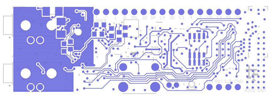
The PCB Design
PICO DSP is a four-layer PCB design. As you can see from the gerber files pictured below, the PCB is quite densely populated and there isn’t much additional space available when both components and trace routing are considered.
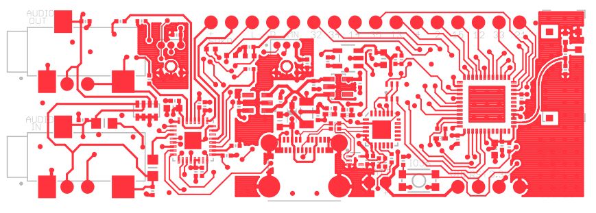
The PCB top layer is for signals, with a few copper polygon pours of power and ground signals.
The bottom layer is also for signals, with some copper ground plane pour at the audio inputs and outputs.
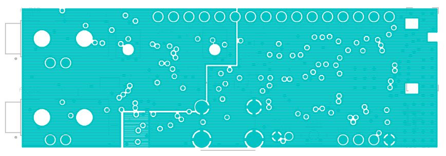
One of the inner layers is for the 3.3V power, the plane is split into analog (VCC) and digital (VDD), and the other one is the ground plane (pictured). The ground plane is also spilt into two sections, analog and digital, and the ground planes are joined underneath the ADC input of the audio codec.
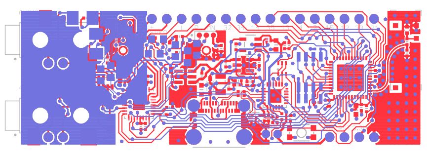
Both the top layer and the bottom layer signal planes.
Stay tuned for our nexxt update where we’ll answer some of your frequently asked questions.