Project update 3 of 15
Memory Benchmarks
In this update we explore the information presented in the memory bandwidth graphs, and explore the performance of POWER in more detail.
A Primer in Computer Memory
Real-world computer performance is a complex function of many different factors, including microarchitecture, core design, cache structure, cache capabilities, and memory controller design, among many others. Cores with otherwise excellent performance have been rendered slow in real-world tasks due to poor design and/or implementation of any one of these areas. As a result, it is important to probe the limits of each CPU implementation in as many ways as possible to determine the real-world limitations of the computing device.
Overall memory bandwidth is a relatively simple way to test how quickly data can be read and written by the CPU core itself. If the memory and I/O controllers are able to keep the cores fed with data at all times (thus avoiding core stalls), then each CPU would remain at or near peak performance continuously. In the real world, this purely core-bound behaviour is almost never realized. Data generated by the core needs to be written to temporary or permanent storage, and the core also needs to read in new data from temporary or permanent storage to continue doing useful work. The memory and I/O subsystems run at a small fraction of the internal core processing speeds, and stalls are largely inevitable.
All modern computers contain multiple levels of read-write cache in an attempt to counteract this problem as much as possible. The cache memories run anywhere from near or at core speed to many times slower than the core, with the larger caches moving further down the cache hierarchy and running at slower speeds. In fact, main memory (DRAM) itself could be looked at as a large, relatively slow cache level directly above the permanent storage devices (hard disk, SSD, etc.). To make matters worse, each cache level down the hierarchy typically has a higher read latency value, Read latency introduces delay from the core requesting a data value to actually receiving the data value, causing core stalls where the core is unable to continue computations. Many benchmarks either repeatedly read and write from a tiny section of memory, in effect only testing L1 and possibly L2 cache speed, or they attempt to stream large chunks of data in sequence from memory, thus only testing the maximum possible transfer rate from main memory under ideal conditions.
Interpreting Memory Bandwidth Graphs
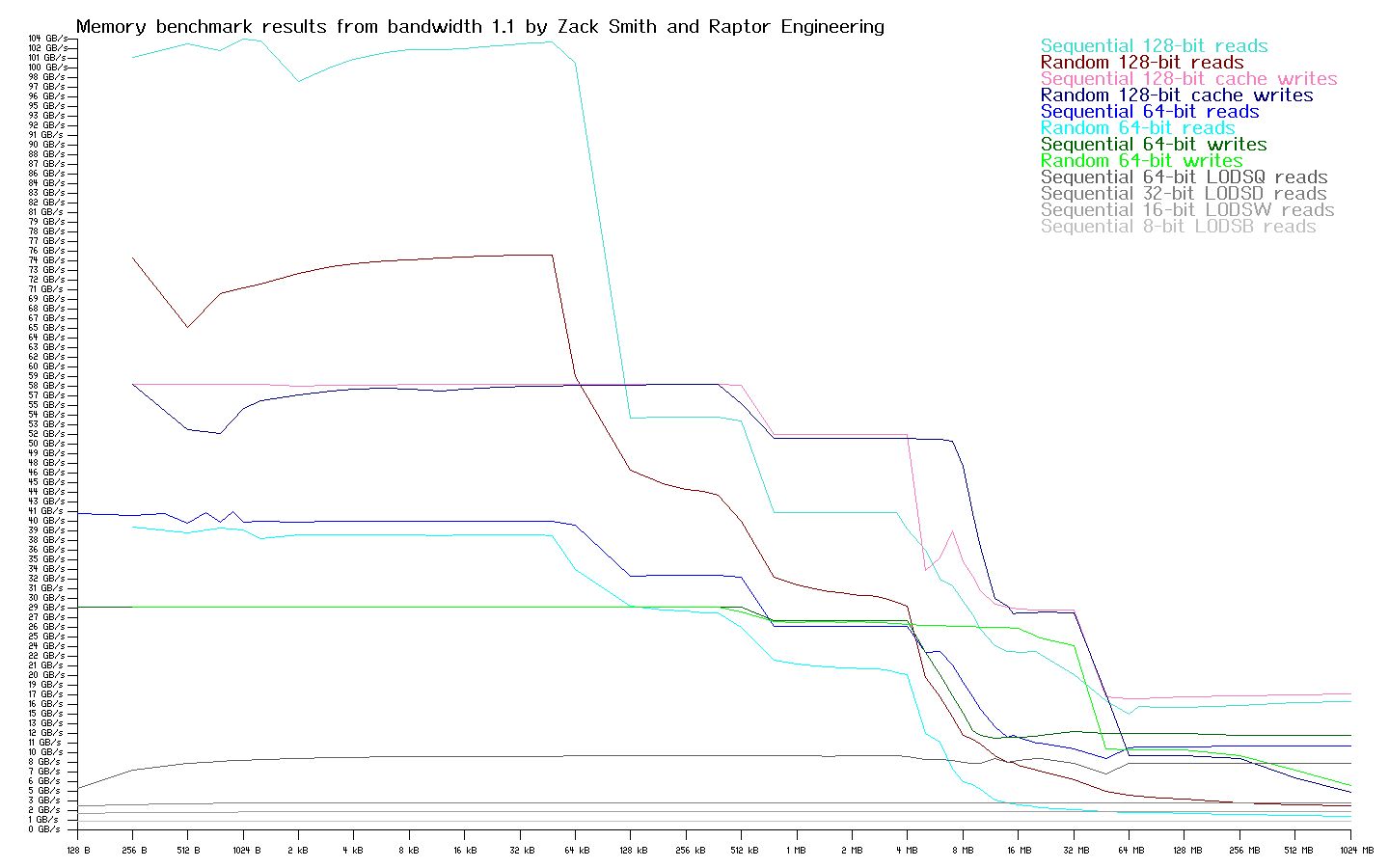
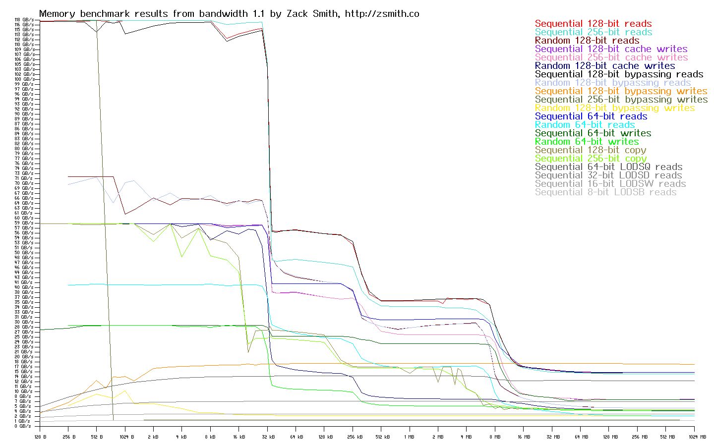
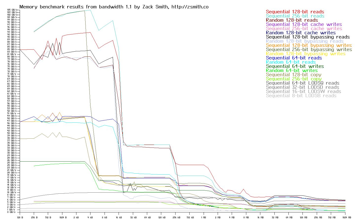
The memory bandwidth graphs below are generated by attempting to read and write continuous and random streams of data from a buffer of a specific given size. The size of this buffer is varied, and the data transfer rate versus buffer size is plotted on a graph. At extremely small buffer sizes, the entire buffer is contained within the fastest cache in the system, the L1 cache. The reported numbers on the extreme left hand side of the graph show the maximum possible data transfer rate as dictated by core design and implemetation. As the buffer size is increased, it begins to test the effective transfer rate of the L1 and L2 caches combined. This is the first sharp fall-off in transfer rate as you read the graph left to right. Eventually, the L2 cache space is exhausted and the combined performance of the L1, L2, and L3 caches (where an L3 cache is present), is tested, yielding another drop off in performance as the slower L3 cache retains the bulk of the test buffer. Finally none of the caches on the CPU package can store the entirity of the ever-increasing test buffer, and the L4 cache / main system DRAM starts to be tested directly. As the percentage of buffer stored in DRAM versus the CPU caches rises, the transfer rate levels off and remains largely steady, reflecting the native DRAM and memory controller transfer rates as the test buffer increases to 1 GB on the far right hand side of the graph.
Streaming performance does not tell the whole story, however. Many real-world workloads use relatively random access patterns, and request latency starts to dictate the maximum achievable read transfer rate in these scenarios. DRAM in particular, while able to achieve a very high stream transfer rate in DDR3 / DDR4 systems, still suffers from basically the same random read latency in terms of nanoseconds as the original DRAM devices from many years prior. As core speeds have increased, and the number of core cycles wasted while waiting for DRAM to respond has increased proportionally; DRAM random read delays have extracted an ever-increasing toll on system performance. You can clearly see the random read bottleneck on all three systems on the graphs; this bottleneck keeps random read transfers at a tiny fraction of the equivalent stream bandwidth once most memory access is targeted at DRAM exclusively.
POWER8 in Talos™ configuration @ 3.32 GHz
Intel® Xeon® E3-1270 "Sandy Bridge" @ 3.5 GHz
AMD® Opteron™ 6328 @ 3.2 GHz
Benchmark Results
It can be directly seen from the graphs that while POWER is core-bound and somewhat slower than Xeon CPUs at the smallest buffer sizes, POWER really starts to shine in comparison with both x86 systems as the test buffer exceeds 32 kB. The large caches and well designed memory controllers postpone the worst DRAM bottlenecks until the test buffer has reached over 32 MB in size, whereas the Opteron systems really start to see performance penalties with buffers of more than 1 MB. The Opteron scores very poorly once DRAM access becomes dominant, while the non-libre friendly Xeon is nearly able to keep pace with the dual-Centaur POWER system in that region.
Many real world workloads, such as software development, GPU-intensive tasks, and virtual machine hosting, will benefit from the large caches, high memory bandwidth, and high I/O bandwidth of the POWER systems. In fact, this is likely one factor in POWER’s ability to run continuously at or near 100% load without the random, severe latency spikes that are often seen under similar conditions on x86 machines. When run in this load region, POWER is very competitive in terms of performance per watt as compared to x86 systems. Conversely, POWER’s peak core performance may be limiting for workloads that rely more on very tight loops that can be retained in the L1 or L2 cache of an x86 CPU, and are not as sensitive to memory bandwidth. Such tasks tend to include small compute kernels, video encoding, and related work. Overall, x86 and POWER are very competitive with one another in terms of performance when tailored to their best workloads, and they are close enough in overall performance that the decision to use one over the other must be made on a case by case basis. As a result, purchasing decisions must be made on the grounds of workload and desired level of security — one platform has severe freedom and security drawbacks, while neither platform shows massively superior performance compared to the other on all possible workloads.
Coming Up: Kernel Compilation
Stay tuned for our next update, where we will compare the software development time of the most powerful libre-friendly x86 hardware available against the performance of a single Talos™ workstation! In the meantime, get in touch if you have any questions or suggestions for future updates.