Hello everyone,
Thank you for signing up and backing this project!
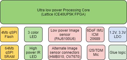
We will delve into the hardware components of the Vision FPGA SoM in this update.
Hardware
FPGA
The SoM is designed around the Lattice iCE40UP5K low power FPGA. This FPGA was chosen for the following reasons:
- Low power consumption, typically in the mW range
- Reasonably sized: sufficient to process images, audio etc. and also map a RISCV processor into it!
- Toolchain and community support: the iCE40 FPGA is well supported in the community by various tools.
Imager
The SoM is designed to support 3 different image sensors:
- Himax HM01B0: This is a low power, rolling shutter color qVGA (320x240) sensor.
- Pixart PAJ6100: This is a low power, global shutter monochrome qVGA (320x240) sensor.
- Omnivision flex: Various low cost sensors conforming to this de-facto standard are available.
Of the three, the Himax was chosen based on user feedback from a survey. The Pixart sensor is not installed and will be made available as an option at some point in the future depending on user requirements.
Microphone and IMU
An Knowles I2S microphone SPH0645 was chosen as the microphone as the I2S protocol is very easy to de-serialize in the FPGA with minimal logic as compared to using PDM where a larger number of microphones are available. Motion sensing is supported by an Invensense ICM20689, a high quality 6DoF IMU meant for Drones, IoT and VR applications.
Memory
qSPI was chosen as it offers ~4x the bandwidth of SPI. The 4Mb flash can store multiple FPGA images as well as code for a RISCV processor or AI models. The generous 64Mb qSPI SRAM SRAM can store temporary data such as images from the camera that may not fit into the FPGA which has a limit of 1Mb.
LED’s
Whats a board without some blinking LED’s? A 3 color LED can be used as for a user interface. A high power IR LED on the SoM can be used to illuminate nearby objects for the camera and also as a presence detector by measuring the image sensor average output with the LED on vs. off. The LED operation is synchronized to the image sensor exposure to minimize power dissipation.
Power
Only a single 3.3 V supply is required to run the module. All required voltages are generated on-board using LDO’s. The 1.8V and 1.2V voltages are brought out to pins for use by the rest of the design (<100mA).
Glue logic
The glue logic enables programming the FPGA and on-board Flash.
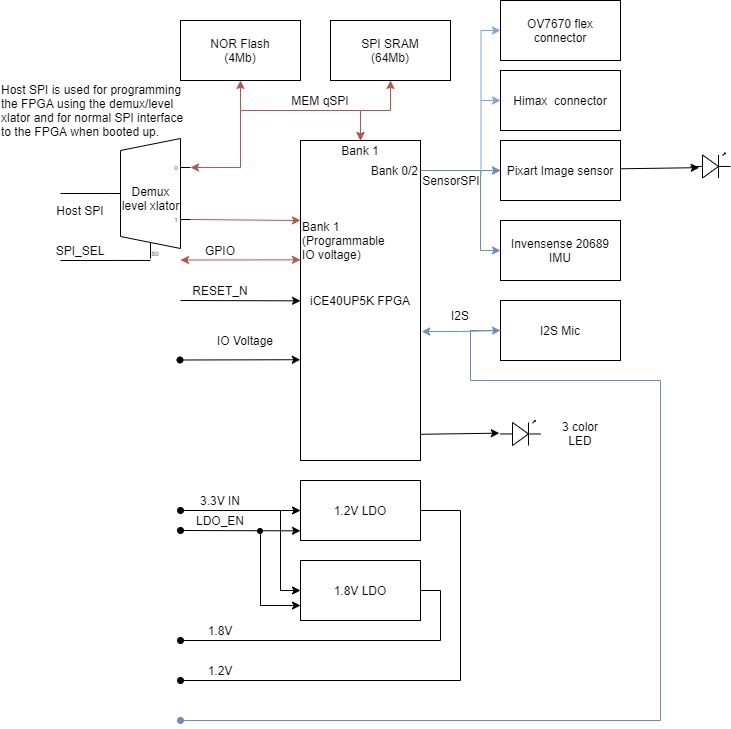
The drawing above shows how the various HW components are hooked up in the SoM. All devices on the SoM operate at 1.8V and occupy two of the 3 banks of the FPGA (Bank 0, 2). The image sensor communicates with the FPGA using I2C (Himax, OV) or SPI (Pixart) and an 8 bit parallel data bus. The sensor I2C bus is shared with the IMU and is also brought out to pins in case the user would like to access these device or for expansion to other sensors.
The memory is on its own dedicated 1.8V qSPI bus with independent chip selects to select the Flash and SRAM.
The glue logic is a bit more interesting: The SoM was designed to look like a SPI slave peripheral to a host processor while allow for flexible voltage levels (using Bank 1 of the FPGA).
- The internal Flash is accessible over the same host interface as that used to communicate with the FPGA making the interface rather simple to implement. An additional chip select is required from the host to enable this functionality.
- FPGA SRAM programming: The FPGA normally boots from the onboard flash on coming out of reset. The Flash can be programmed by the host as indicated above. However, this process of programming the flash can take a significant amount of time (20 seconds). The FPGA SRAM (also known as CRAM) on the other hand, can be programmed in about 60ms, enabling fast turnaround of bitfiles. This feature is available using a dedicated input and is transparent otherwise to the user.
- Host interface: The host interface to the FPGA is over a 4-wire SPI with 4 uncommitted IO. The voltage levels on all 8 pins is fully programmable using an external voltage. This enables a glueless interface to pretty much any host.
PWB
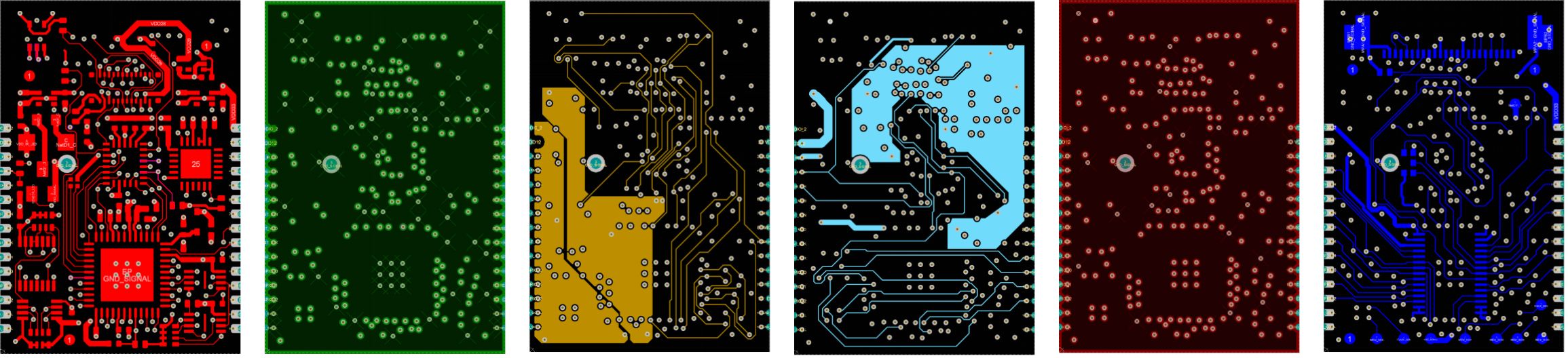
The PWB is a 6 layer board that was designed using Altium. The initial designs were using 4 layers but when the various sensors options were added, this resulted in requiring 2 more layers to successfully route the board. Castellations were added to make the board easy to solder into a system board. However, this required that all parts be placed on the top side. With the exception of the microphone (bottom ported) and the connector, this was possible. Solid decoupling has been provided along wiht a solid ground plane and dedicated power planes for the best possible power distribution to the various devices.
Toolchain
- Proprietary: The SoM is fully compatible with the Lattice Radiant toolchain. This is required for supporting the AI flow as the SensAI core is delivered encrypted by Lattice.
- Open Source: The icestorm toolchain is not only open source and freely available, it produces excellent quality of results which for a small FPGA is important. Both Verilog and VHDL are supported for programming in addition to various other higher level languages and frameworks such as APIO, icestudio, Python, LiteX.
Talk to us!
The project is not yet buttoned up! A lot of work remains in terms of software, documentation, marketing, training framework, hardware verification and so on. We invite you to collaborate using the Crowd Supply Discord channel and/or the tinyVision Discord channel.