Project update 15 of 15
Dev Edition and Probes Shipping Soon
by Aleksa BHi All,
I’m pleased to announce that dev edition units and all probe kits will be shipped out in a few weeks time! So now would be a good time to verify your shipping address on Crowd Supply to make sure you get your order when we ship it. Now that I’ve got the big headline news out of the way, we can get into the details of how we finally got here.
Rev 5.3 Hand Build
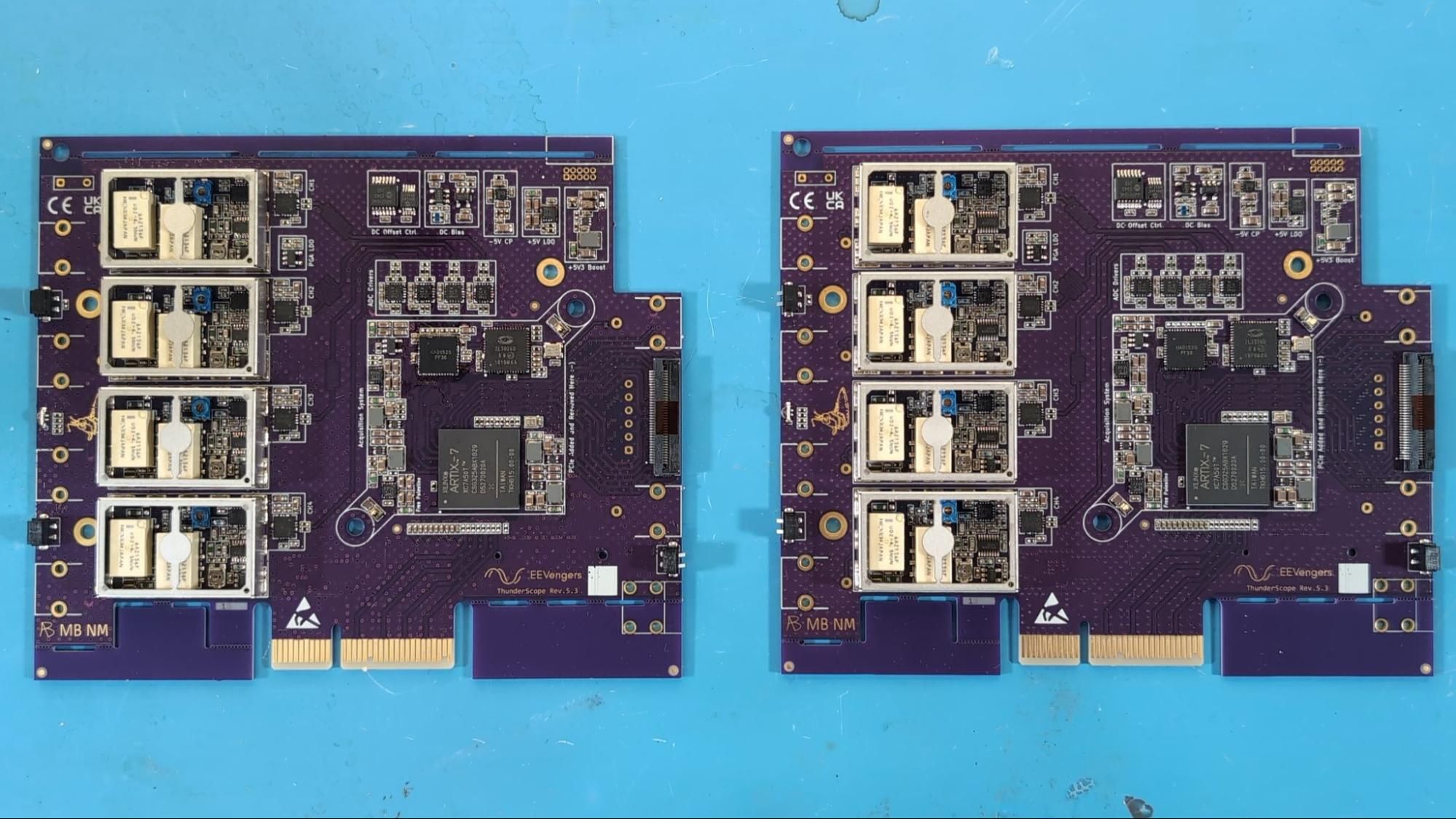
While waiting for quotes from some CMs (one of whom gave me the run-around for over a month), I decided to do a quick hand build of 5.3 to iron out any issues with the new ADC driver circuit.
A New LDO
My main concern with the ADC drivers was the added current draw on the 3.3 V LDO in the acquisition system. I was glad that I did the hand build when I found that the 300 mA rated LDO on the initial 5.3 design was sourcing up to 335 mA! I then tested a few drop-in replacement parts and selected a low noise 450 mA rated one to use on the production run.
Revisiting the Bandwidth / Noise Trade-Off
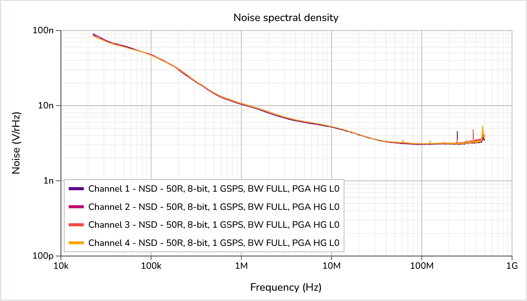
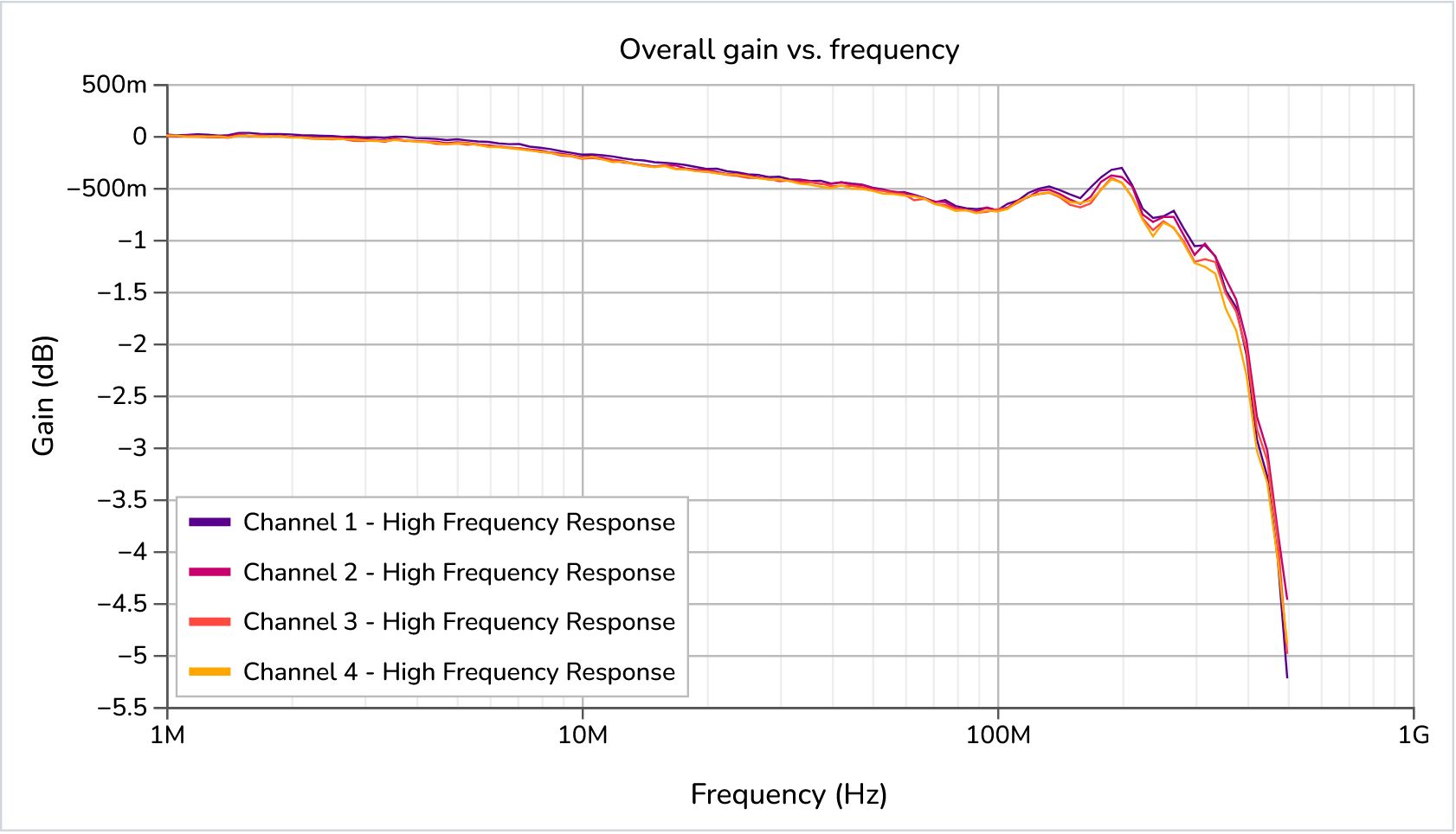
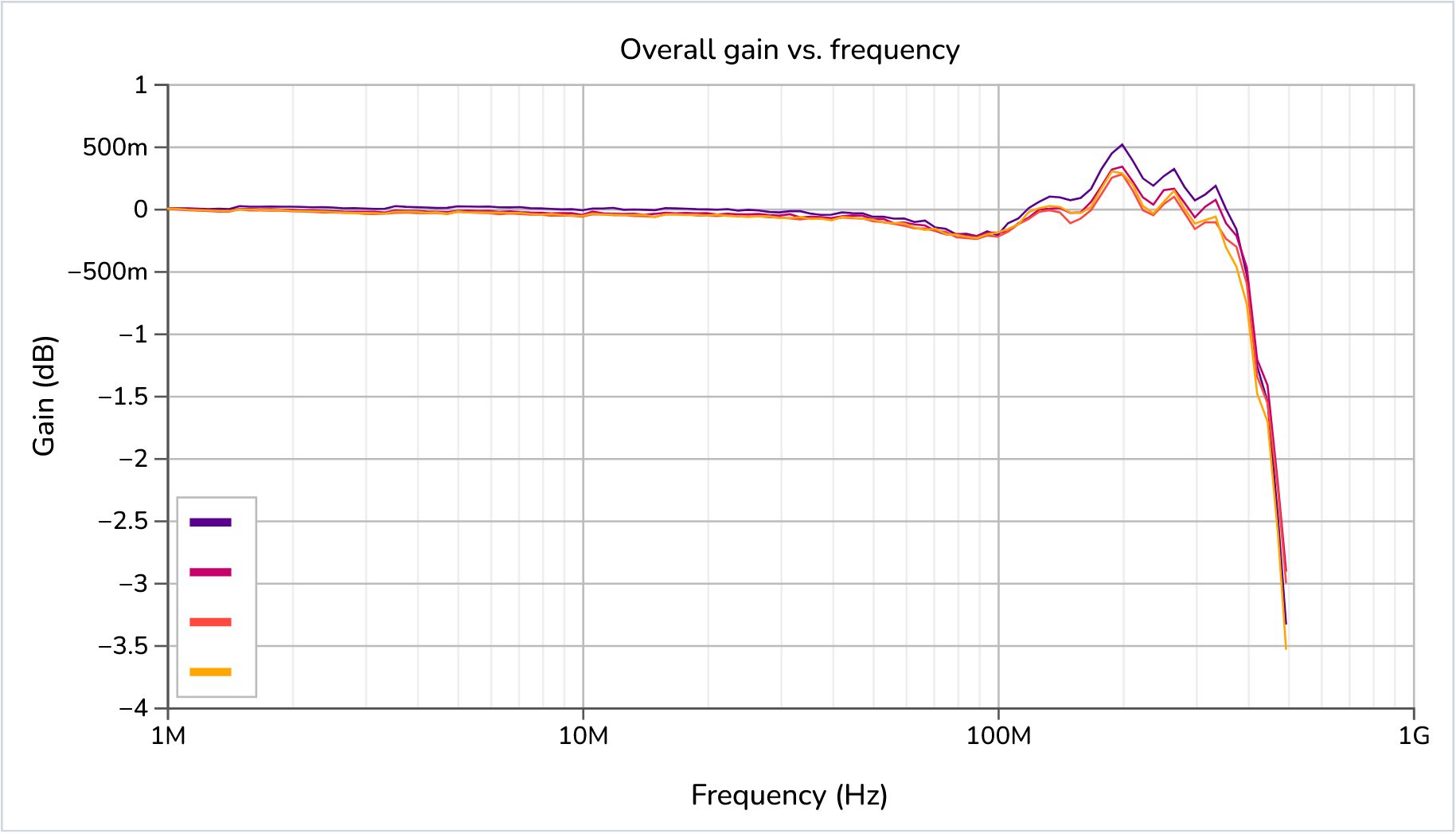
As built, the noise measured 87.0 uVrms with a bandwidth between 400-450 MHz. The noise spectral density and frequency response of the unit is shown below:
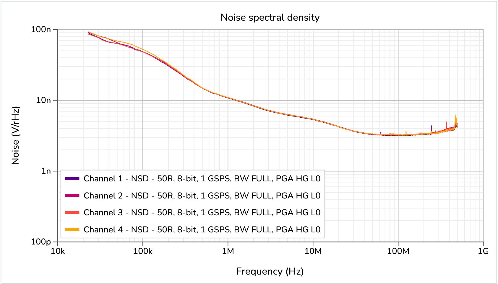
I got annoyed at these results and decided to hit 500 MHz after all, trading off noise a tiny bit more. This just required a change of adc driver output resistor, and after a couple tries I found a value that reliably hit 500 MHz of bandwidth with 93.8 uVrms of noise. The noise spectral density and frequency response of the modified unit is shown below, and should be indicative of a production unit.
Smoke Testing the First Batch of PCBAs
After a lot of painful logistics work, the assembled boards arrived. I had to send the CM the stock of ADCs I had in inventory instead of using the new parts I had ordered directly from Analog Devices. This was because the order needed export approval to ship to the CM in Shenzhen, which I was advised could take a few months (and we are still waiting at time of writing!).
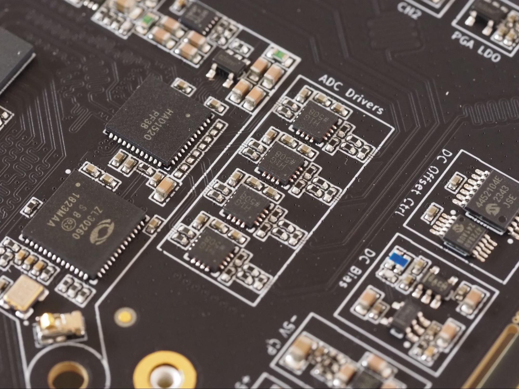
I was pretty worried about the failure rate of these parts, so I got to work building up and testing every board to figure out how bad it would be. Turns out, not too bad! Only 6 units needed an ADC replacement to have enough to ship out all the dev editions. This lets us get something out the door while waiting for the US department of commerce to let me, a Canadian, have the Norwegian designed parts delivered from their country of origin of South Korea to my CM in China. If we do get approval then the next batch will use fresh new ADCs, if we don’t then we’ll have to figure out some other way to buy the chips and get them to the CM!
Defusing a BOM Issue
I was really excited to get the pictures of the assembled boards before they got shipped out to me, they were finally real and looked really good to boot… Until I looked closer at the front end. Turns out the CM had used the wider UD2-4.5NU relays, rather than the compact UD2-4.5NUN relays specified in the BOM.
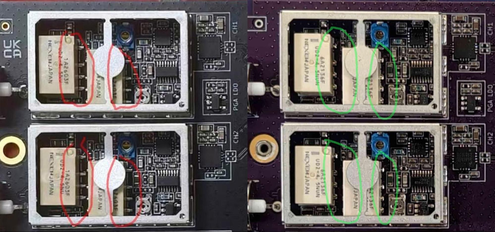
I confirmed that they did in fact swap them without asking me first. I asked if they could rework them and they brought up concerns with damaging the rest of the components under the can, as it is a tight squeeze. So I told them to test each board for shorts to make sure none of these very close together pins were touching due to variation in soldering. X-rays came back clean so I told them to go ahead and ship them. I was very worried about the hit to voltage clearance (40V isn’t a lot but still) and potential hit to performance so I figured I could use a pair of very fancy flush cutters to trim the leads. That route didn’t work too well so I made a custom chisel tool for the job:
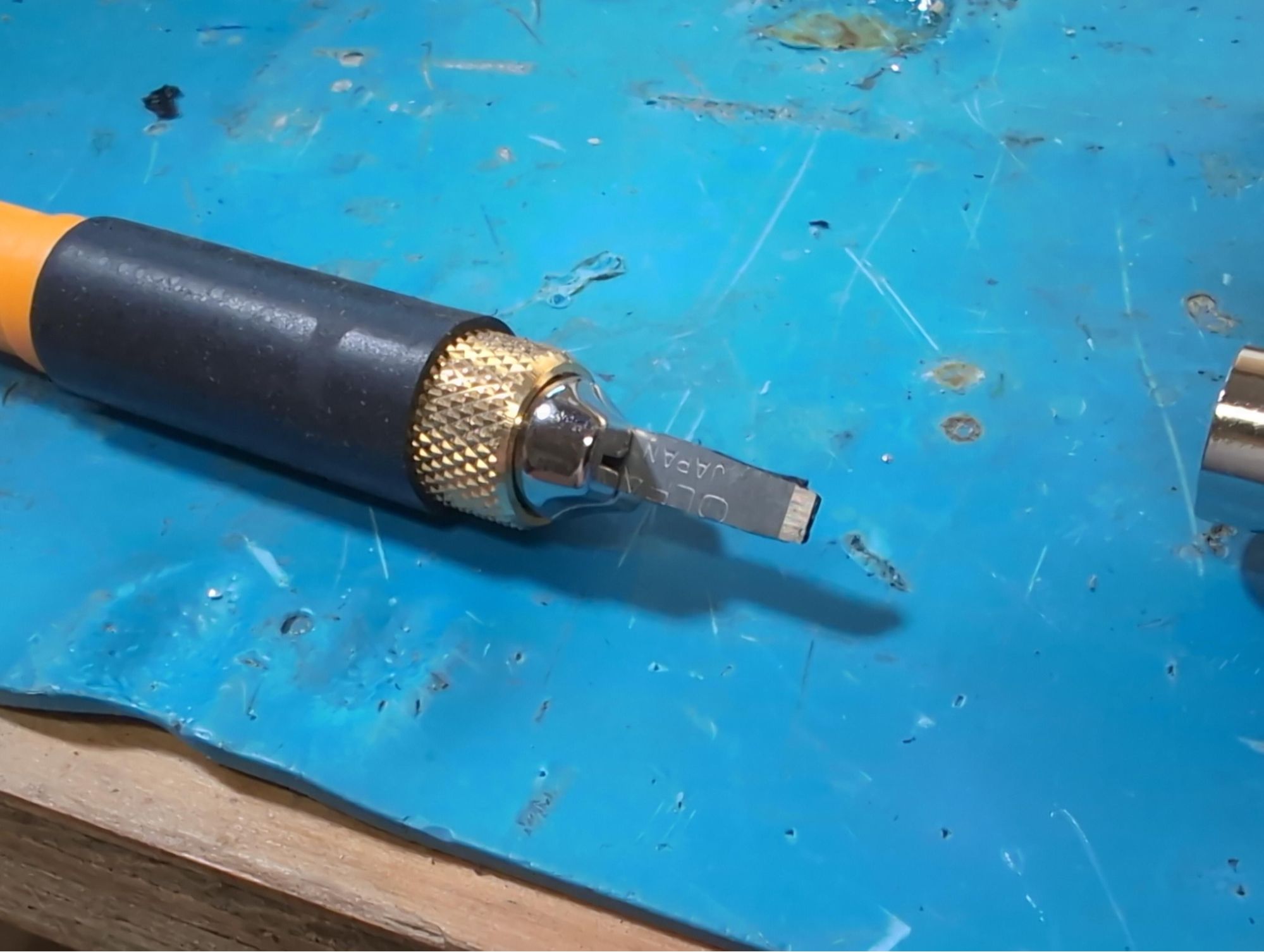
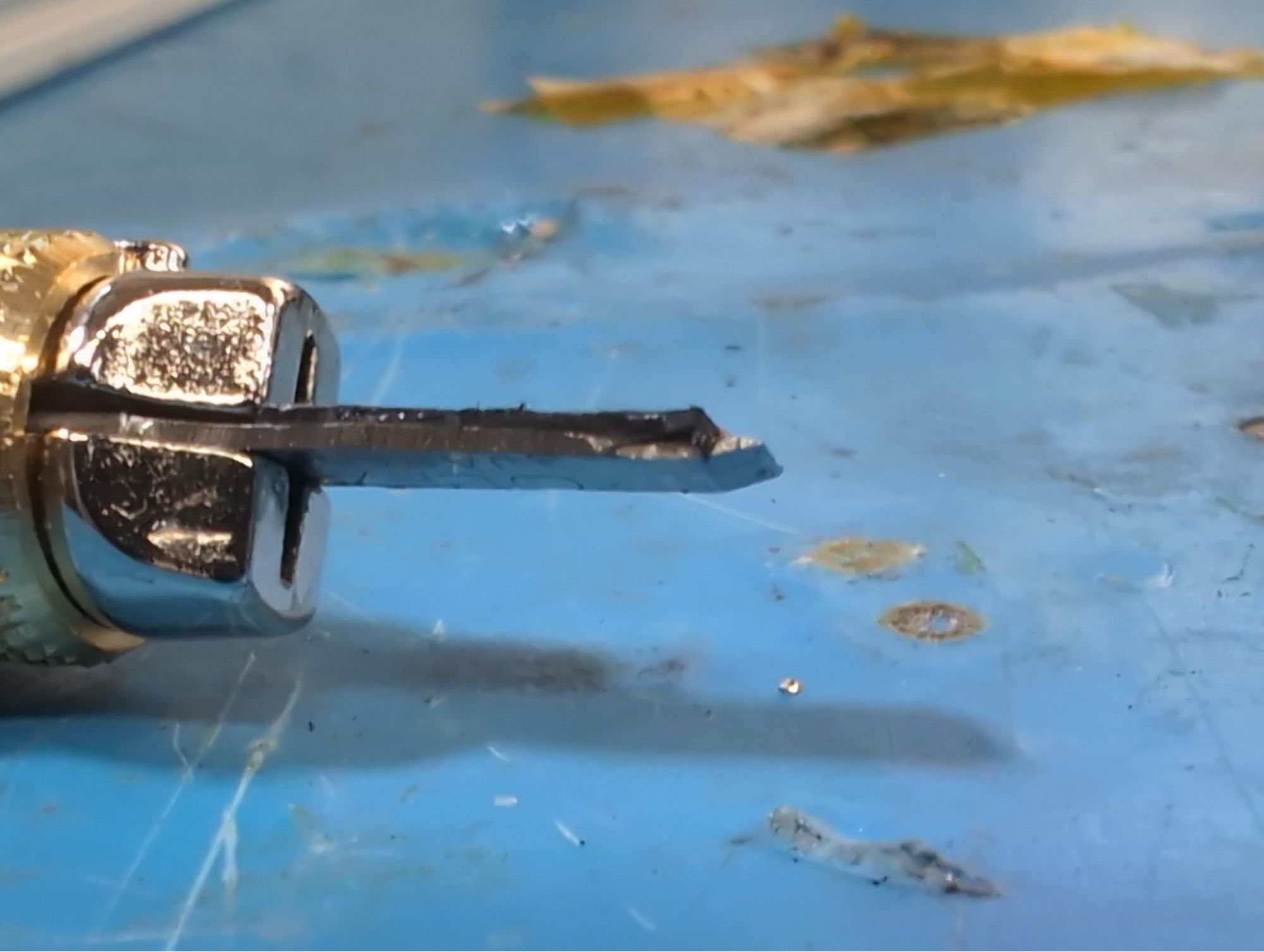
The idea here is to shim the one end of the blade so that it can be inserted flush with the relay, positioning the cutting edge perfectly to be able to push down and trim the excess length of the pin. This does work well but is tedious, so I will be doing a few tests to see if the longer pins actually cause any issues or not. To be honest, this bothers me so much I may power through and trim all the leads regardless. If only the one manufacturing issue wasn’t in the front end that I spent years fussing over! At least this won’t be a problem for the next batch, we do production validation testing (PVT) runs before mass production for this exact reason.
Build Status and Timeline
At time of writing, we have all the probes packed and all the PCIe units fully built and in the process of calibration. Here’s a couple glamour shots of the first PCIe unit to get its custom milled and engraved bracket installed:
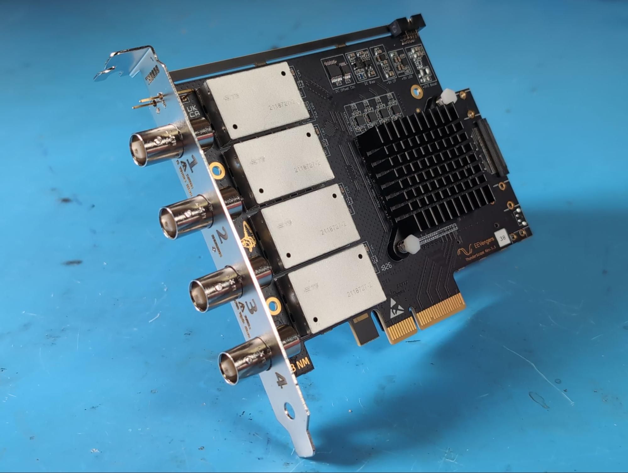
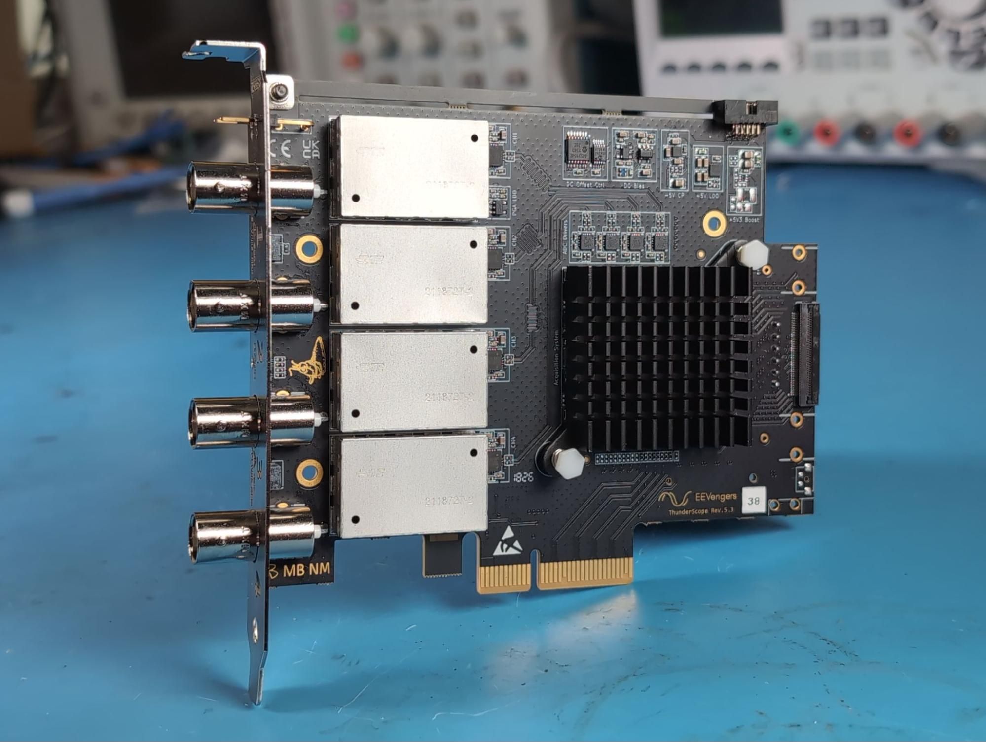
As for the USB4 units, we have all the main board assemblies and end caps ready for box build, which is what we will start on once the PCIe units are done and packed up. As mentioned at the start, these last steps should only take a few weeks at most. I’ll send out an update once we ship to Crowd Supply, but until then it’s back to the assembly line for me.
-Aleksa