Project update 3 of 5
QUARK's Operational Scheme
by Ismulin M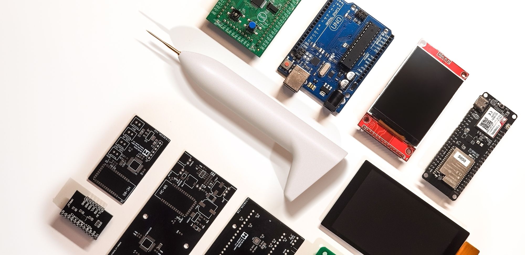
QUARK is based on the ESP32 controller. It uses a ready-made ESP32-WROOM module. All the main tasks for the implementation of operating modes, calculations, screen drawing, wireless connections, are dealt with by the ESP32. Also, QUARK has an Atmega328 on board, which acts as an additional ADC when digitizing signals in oscilloscope mode and sets the sensitivity of the input op-amp. In addition, the Atmega328 multiplexes the resistor array when measuring resistance and capacitance, and performs the secondary functions of turning on the board backlight LED and sending sound to the speaker. Let’s look at this in more detail:
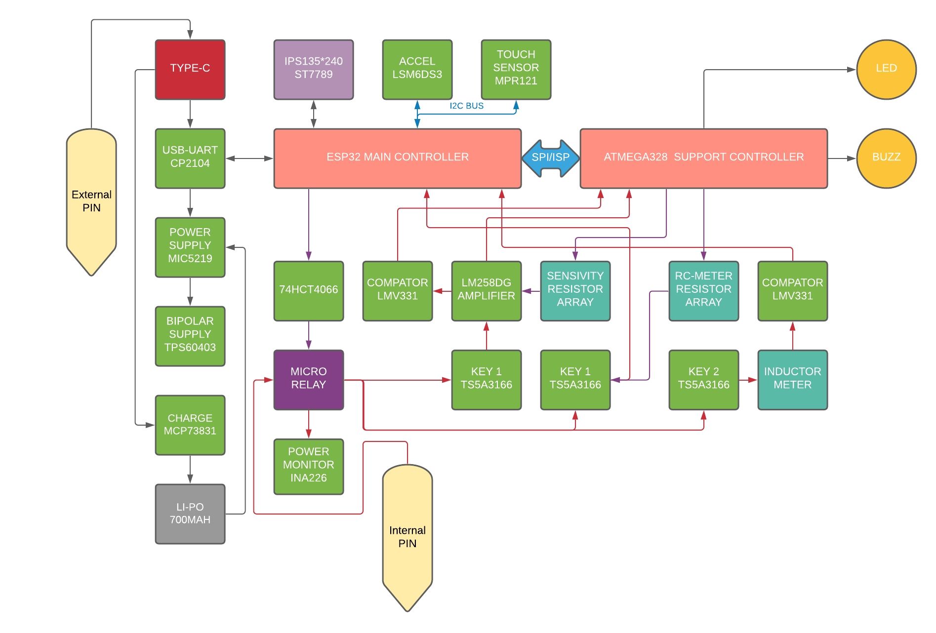
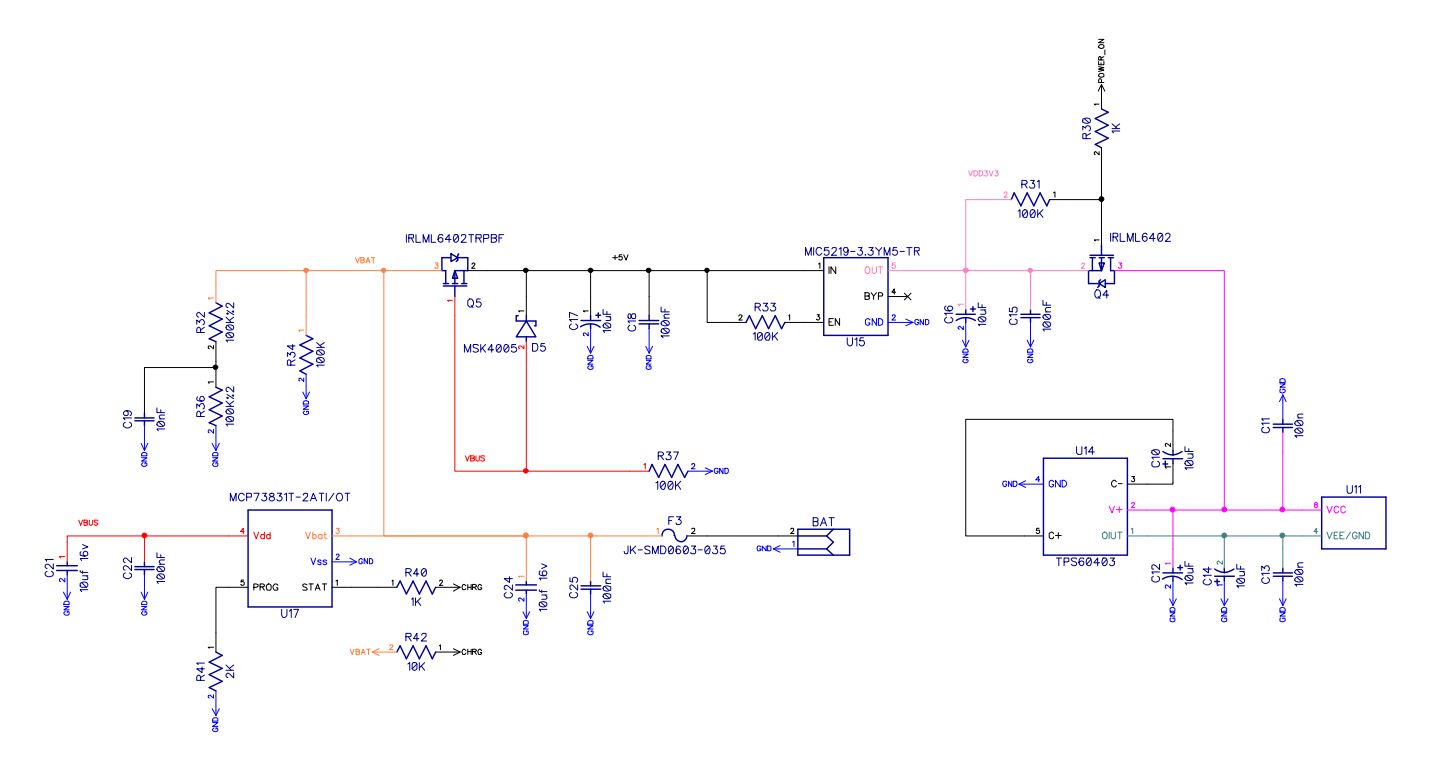
The external probe (External PIN), plugs into the TYPE-C connector. In the standard configuration, it is connected to the ground of the device and all measurements are made relative to it. Through the same port, the device is charged using the MCP73831 micro-circuit. The stabilized power supply is provided by the LDO MIC5219, and the TPS60403 electronic pump which implements a bipolar +/- 3.3 V power supply to power the op-amp of the oscilloscope input stage. Below is a diagram describing the power supply of the device:
Data exchange is implemented over TYPE-C via the USB-UART bridge on the CP2104, with the main controller provided by the ESP32 and Atmega328. Moreover, for communication between the computer and the Atmega328, the ESP32 acts as a translator, since the Atmega328 is not directly connected to the CP2104. For example, in order to upload the firmware to the Atmega328, the ESP32 is switched to ISP-programmer mode and the data is uploaded via the SPI bus. On the same bus, the ESP32 and Atmega328 communicate with each other in operating mode.
The built-in probe (Internal PIN) is connected to the main circuit via a bistable electromechanical relay. In all modes, except for current measurement mode, the relay is in the "Main" state. First, let’s consider the current measurement mode. The relay from the "Main" is switched to the opposite state, while the external (External PIN) and built-in (Internal PIN) probes are shunted through a current-measuring resistor of 0.1 Ohm. In this case, the electronic keys (KEY 1 TS5A3166 and KEY 2 TS5A3166) are mechanically disconnected from the built-in probe. The relay is bistable, which means it consumes current only when switching state and is connected via a multiplexer (74HCT4066), as seen here:
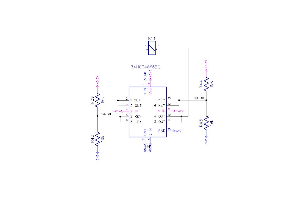
This was done for two reasons. First, the switching current, although small, loads the controller outputs. Secondly, the relay switches with different polarity, which means it is impossible to connect a protective diode, increasing the risk of failure of the controller ports. The inputs and outputs of the 74HCT4066 are cross-linked, and are labeled REL_01 and REL_02 in the diagram. Additionally, by resistors R29 and R43, on the one hand, and R44 and R45, on the other, the inputs are forcibly pulled up to an average undefined state in order to exclude accidental switching.
Consider the operation of the current measurement mode using a piece of circuit as an example:
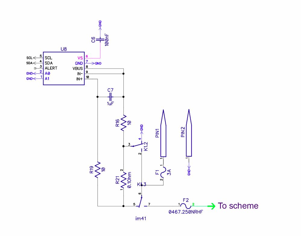
In the PIN1 built-in probe, the relay is in the position shown above. The current flows through PIN1 -> fuse F1 -> contact group 1.3 of the relay -> current shunt R21 -> contact group 1.2 of the relay and out to the ground of the device. The second PIN2 probe is always connected to ground. Thus, the voltage drop is measured from the contacts of the current-measuring shunt R21, through the resistors R19 and R16, via the specialized micro-circuit U8 on INA226 (POWER MONITOR INA226). Data in digital form, via the I2C bus, is sent to the main controller.
In the main mode of operation, the relay contacts are in opposite positions:
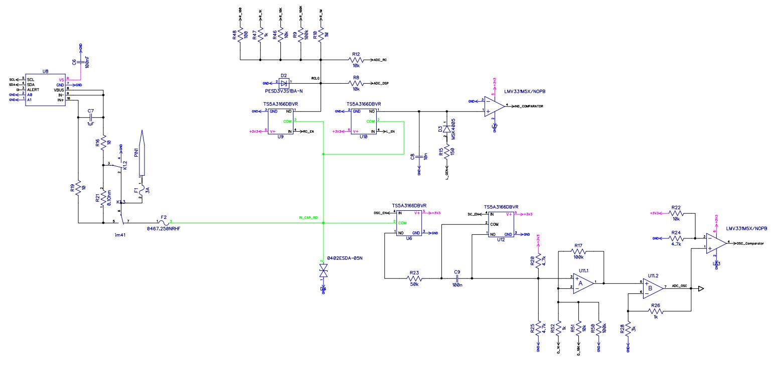
If we need to measure the voltage, then the signal flows from the built-in PIN1 probe, through the F1 fuse, and on to the group of contacts 1.2 of the relay. Then, through the resistor R16, it is fed to the VBUS input of the INA226 microcircuit, on which voltage is measured relative to the ground. As a reminder, the second probe is always connected to ground through the TYPE-C connector. Otherwise, the signal goes through contact group 1.3 of the relay and the superfast F2 fuse. Micro-circuits TS5A3166 electronic keys with ultra-low internal resistance U6 (KEY 1 TS5A3166), U9 (KEY 2 TS5A3166) and U10 (KEY 3 TS5A3166).
In the resistance or capacitance measurement mode, KEY 2 (U9) opens and the array of resistors R9, R10, R46, R47 and R48 (RC-METER RESISTOR ARRAY) is activated. Resistance is measured across a voltage divider formed by the unknown resistance and one of the resistors in the array. For a more accurate determination of the rating, the INA226 ADC is used. The capacitance is measured using the RC time constant method. In the same way, depending on the value of the capacitor, a resistor of a certain resistance from the array (RC-METER RESISTOR ARRAY) is connected and the charging time is measured. Similarly, in the UART-logger, UART-plotter, and signal generator modes, the signal also goes through the KEY 2 (U9) key.
Inductance is calculated by measuring the resonant frequency across the known capacitance C8. In this case, KEY 1 (U6) and KEY 2 (U9) are closed, and the signal goes through KEY 3 (U10). From the controller, a short pulse goes through the protective diode D3 to the capacitor C8 and through the open key KEY 3 (U10) to the measured inductance. The frequency signal is taken from the output of the comparator LM331 (COMPATORLMV331).
In oscilloscope mode, KEY 2 (U9) and KEY 3 (U10) are closed, and KEY 1 (U6) is open. The signal enters the input path executed on the LM258DG op amp (LM258DG AMPLIFIER) (U11.1 / U11.2). Resistors R20 and R25 are zero-shifted. The level of signal amplification is regulated by an array of resistors R50-52 (SENSIVITY RESISTOR ARRAY). R51 and R52 are controlled by the controller. The signal from the op-amp goes to the input of the ESP32 ADC, where it is processed and the trigger, frequency, and period are determined. Further, the data, in a prepared form, is transmitted to a smartphone via bluetooth.
The device is controlled using a specialized microcircuit MPR121Q (TOUCH SENSOR MPR121):
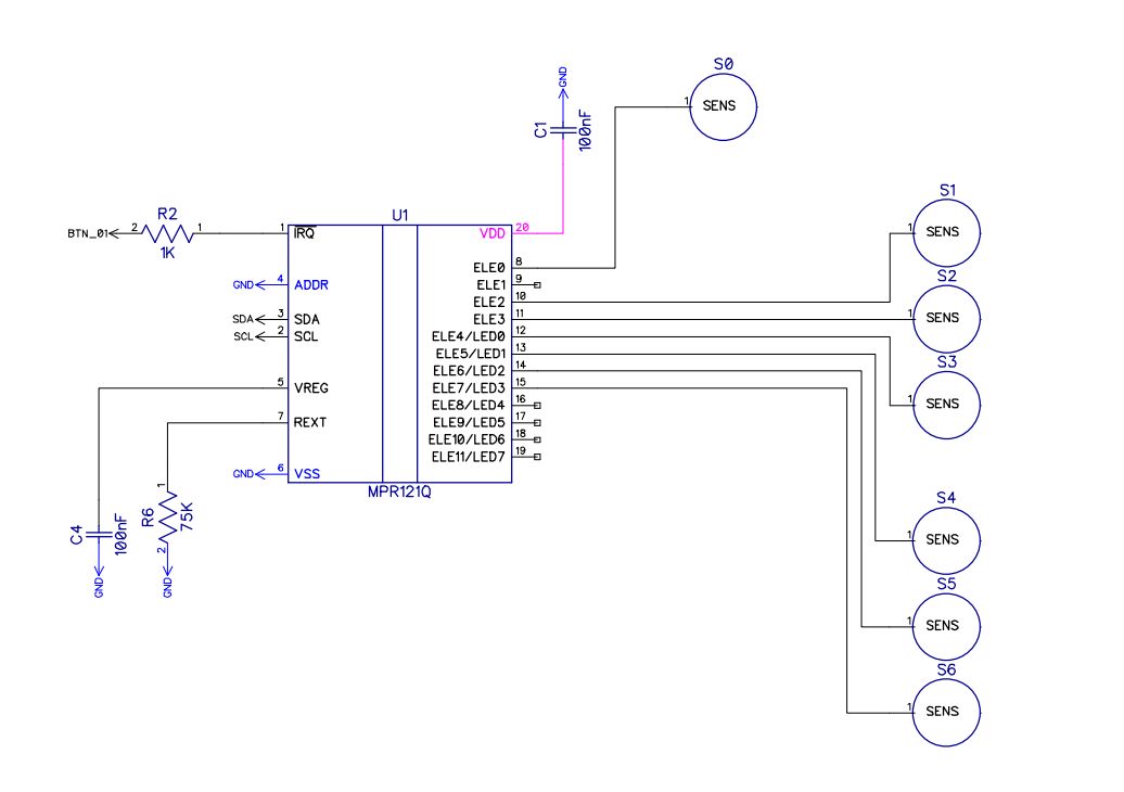
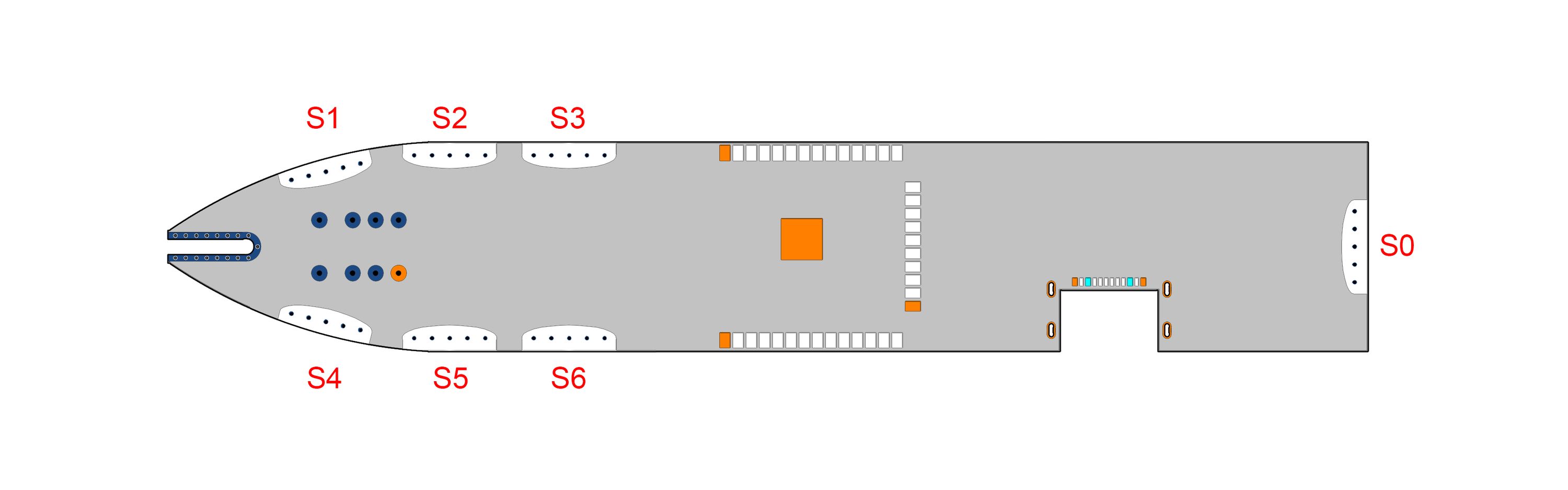
Sensors S1, S2, and S3 are combined into one group, and sensors S4, S5 and S6 into another. This is done so the sensor can be used by both the right and left hand. Only one group of sensors is activbe, oriented to the working hand. Schematically, the location of the sensors is as follows:
The S0 sensor is always functional so it wakes the device from sleep mode using an interrupt signal on the IRQ pin. Since the MPR121Q does not allow hanging an interrupt on an arbitrary sensor, to exclude the occurrence of an event from any sensor before going into sleep mode, the MPR121Q is configured so that there is only one working input - S0. After waking up, the MPR121Q controllers are reconfigured to work with the selected group of sensors.