Project update 4 of 10
Power Capability & Testing
In this update — power testing!
As you may recall from last week’s update, there are a few components between the input power connector and the power rails provided to the downstream USB Ports. Let’s exercise them a bit and see how they fare!
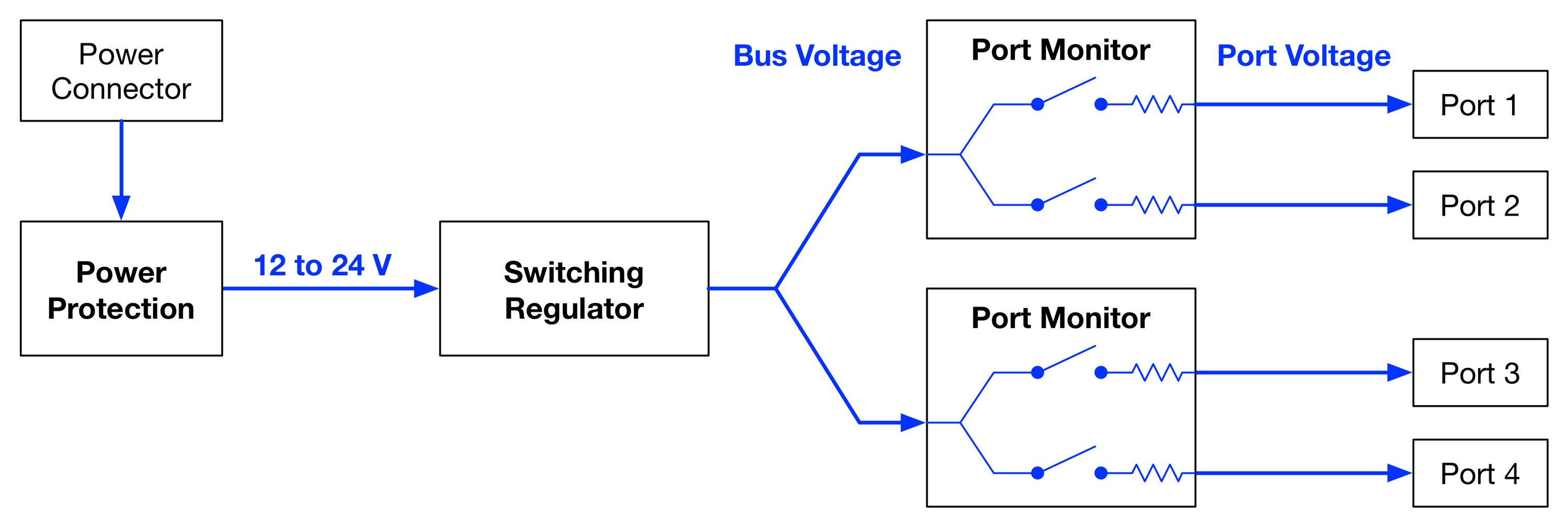
- Power Protection : Over voltage protection, surge protection, reverse polarity protection.
- Switching Regulator : High-efficiency conversion of input 12 to 24 volt rail to 5.1 volts. On the Programmable Hub, the MIC45205 is used.
- Port Monitors : Individually monitors, switches, and limits power provided to each downstream port. On the Programmable Hub, the UCS2113 is used.
Power System Test Hardware
The following test setup was created to test the power delivery and protection capability of the Hub.
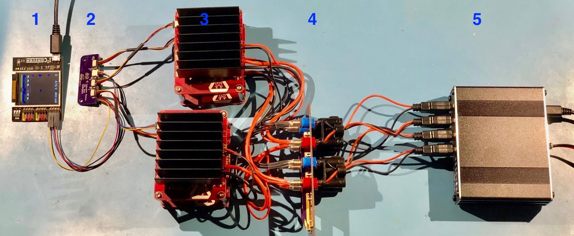
From left to right, it consists of:
- I2C Driver : USB to I2C bridge connected to a control computer.
- TCA9548A Breakout Board : A 1:8 I2C bus switch, allowing downstream I2C buses to have identical devices and addresses.
- 4x Electronic DC Loads : These can operate in a constant voltage or constant current mode, and can create a load of up to 24 V or 3A.
- Interface wiring between DC Loads and USB A connectors
- A Programmable USB Hub under test (commonly referred to Device Under Test or DUT). The Hub is also connected to the control computer to allow the Hub's reported state to be monitored and controlled.
This test setup allows for precise & dynamic loads to be individually applied to each port and the full load capability of the Hub to be exercised.
Bus Voltage Regulation at Load
The first test presented here is a look at the performance of the switching regulator under varying load conditions.
To compensate for downstream voltage losses in external cabling, the Hub’s switching regulator is configured to regulate the 12 to 24 volt input power down to 5.1 volts, instead of the nominal 5.0 volts that the USB specification calls for.
This slight over-voltage is within the standard’s specified bus voltage range of 4.75 volts to 5.25 volts, so there is no chance of damage to downstream devices. In the following graph, this specified range is shaded blue.
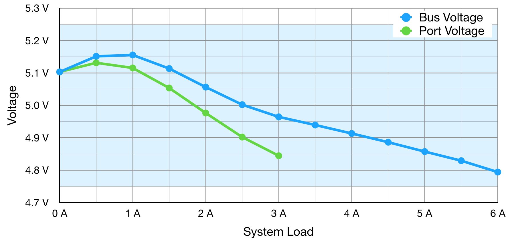
During this test, loads between 0.5 A and 2 A were applied to three of the four downstream USB ports, while the fourth port was used to record Bus Voltage. As you can see, the system does a decent job of maintaining a 5.1 volt bus, and bus voltage only drops 0.3 volts when 6 amps are drawn from the Hub.

It turns out that half of this loss is due to the inherent resistance of the PCB trace between the regulator and the downstream ports. The 1 oz copper of the board has a sheet resistance of 0.5 mΩ per square and the main trace is 100 mm long by 2 mm wide, which results in a trace resistance of approximately 25 mΩ.
The next board revision will have an improved layout to reduce these losses at high system loads.
Note: the initial version of this update had an incorrect main trace length, which exaggerated the losses within that trace. The length used in the calculation was the total length of the +5V rail, instead of just the length of the trace between the regulator and the downstream USB port outputs.
The Port Voltage is a calculated value and shows the effect of the UCS2113’s 40 mΩ internal resistance across its’ load switch and current monitoring shunt resistor.
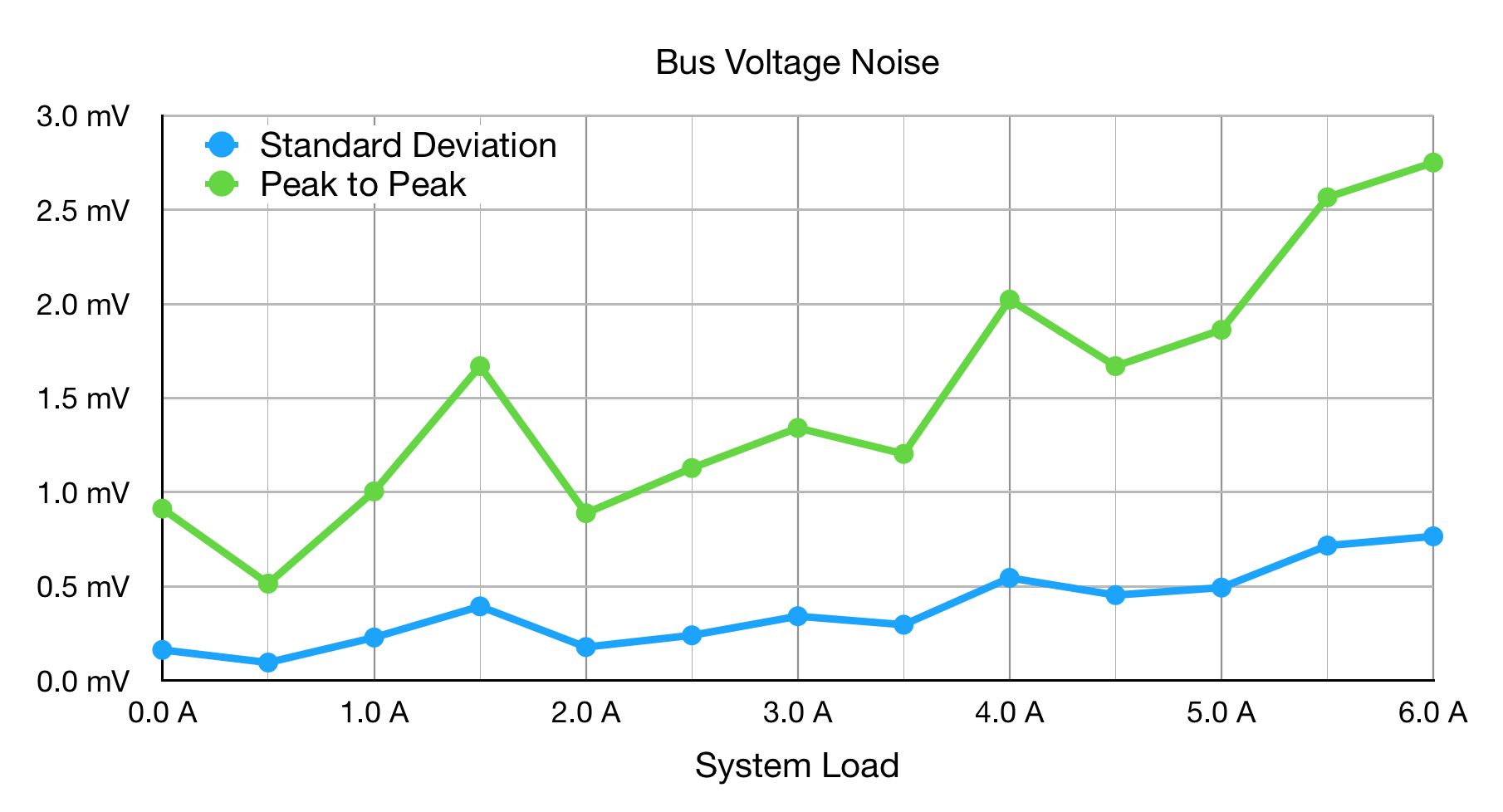
During this test, many voltage readings were taken and the standard deviation and peak-to-peak noise of the bus voltage were calculated.
Both of these noise figures are impressively low. At 6 A of system load, there is less than 3 mV of peak-to-peak ripple on the power provided to downstream ports!
Individual Port Protection
Next up, the individual port protection & monitoring functionality. In this first step, a single port will start with a 0 mA load, and every 5 seconds the load increases by 100 mA until the load reaches 2 A.
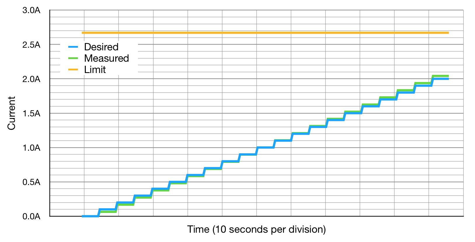
The does not enter any fault state during this test because the port’s limit is set to 2.67 A.
Next, let’s repeat the test but with 2.9 A endpoint to see what happens when the 2.67 A limit is exceeded.
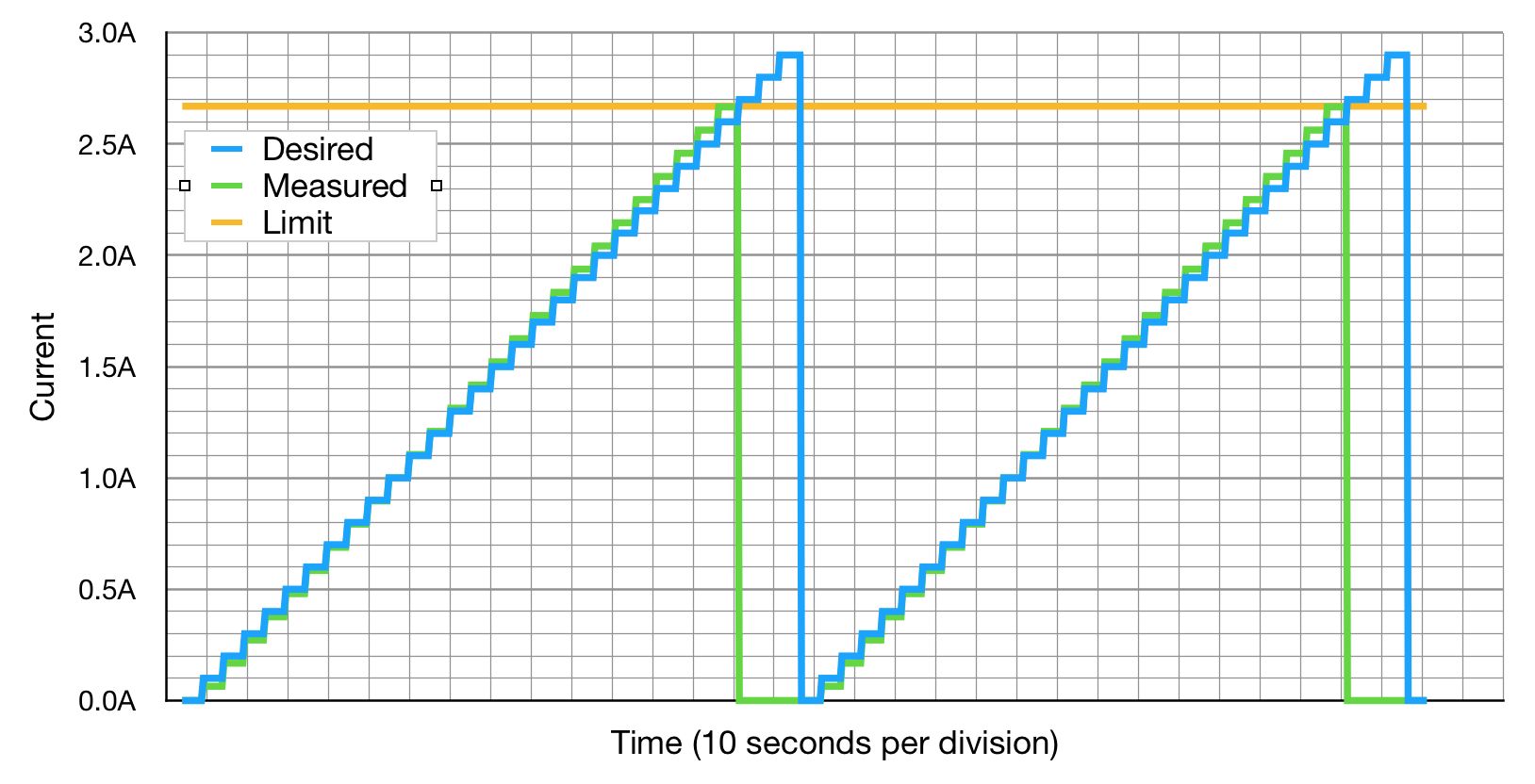
The UCS2113 performs exactly as specified. After the current limit is exceeded, the power to that port is automatically and instantly cut. Once the load is removed (or the port’s power output is reset), loads that are below the limit can be drawn from the port again.
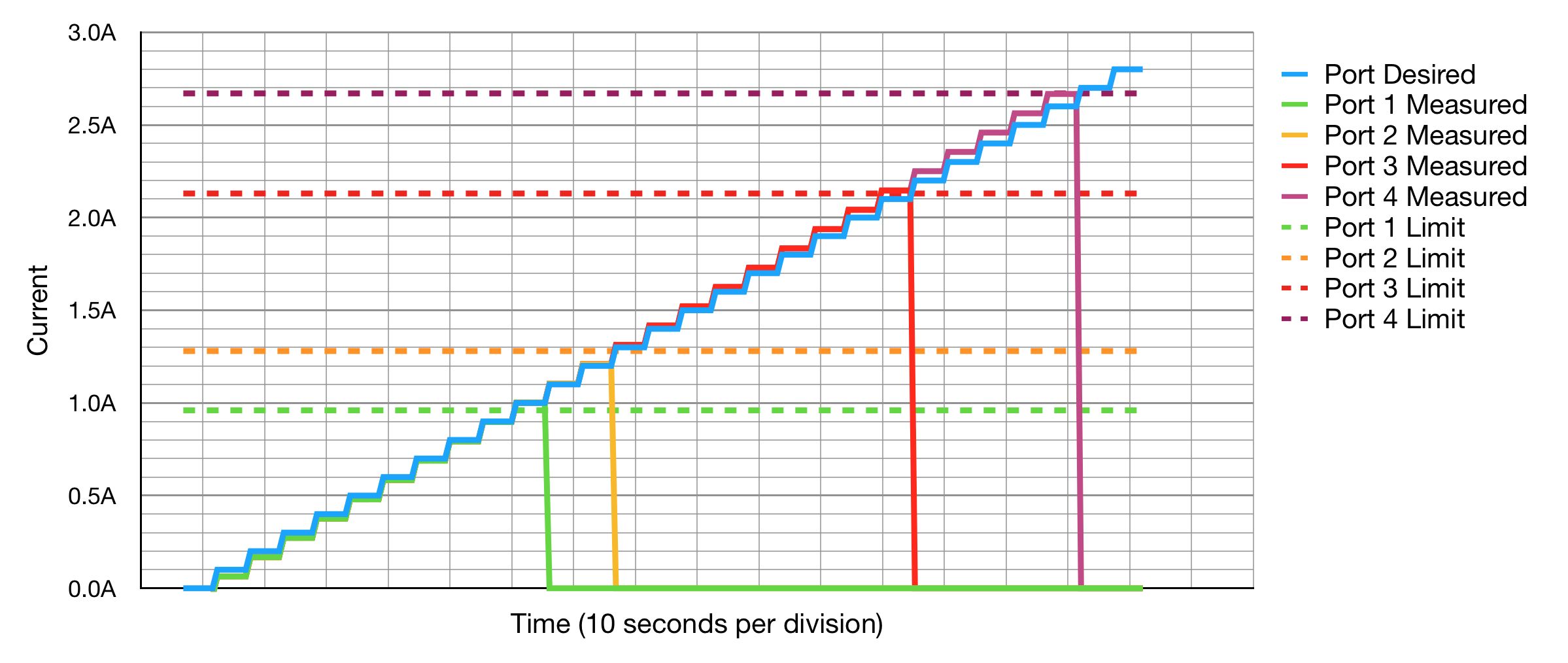
Here, four different current limits are set for the four downstream ports:
- Port 1 : 0.96 A
- Port 2 : 1.28 A
- Port 3 : 2.13 A
- Port 4 : 2.67 A
And the same step test repeated, but all four DC loads are used to draw power from all four downstream USB ports. As you can see, each port’s power is cutoff automatically when its’ current limit is reached and neighboring ports are not effected. There is no cascade or group failure more — each port is configured and limited independently.
For the last test presented this week, the DC load system was configured to pick a random current for each port between 0 A and 2.5 A every 5 seconds over a test duration of 10 minutes. Port current limits stayed at the previous tests’ 0.96 A thru 2.67 A settings. Due to this, Port 1 serviced loads are all below 0.96A, Port 2 loads are all below 1.28 A, etc.
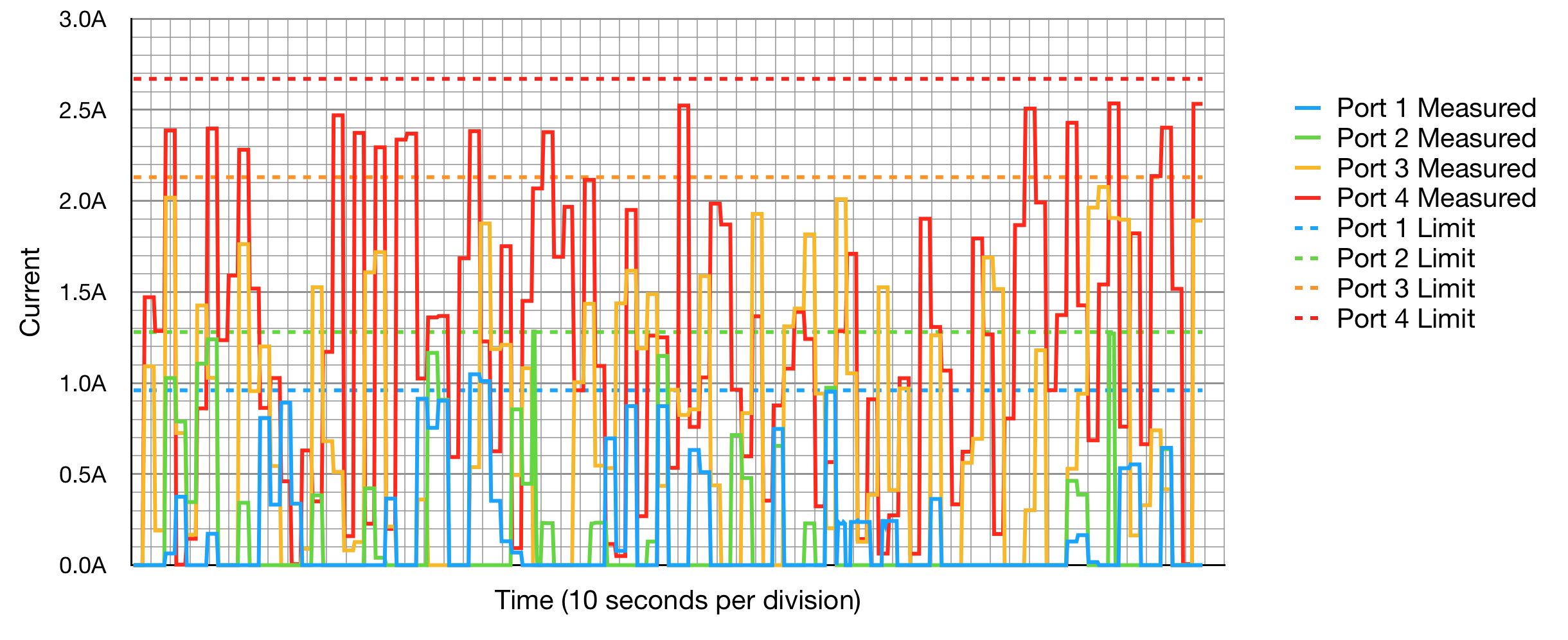
| Port | Average Load | Max Load | |
|---|---|---|---|
| Port 1 | 0.17 A | 1.05 A | |
| Port 2 | 0.16 A | 1.28 A | |
| Port 3 | 0.72 A | 2.08 A | |
| Port 4 | 1.22 A | 2.54 A |
I hope you enjoyed seeing this testing of the Programmable USB Hub’s power system. The test hardware presented here will be making its way to the production test fixture, and will be used to test the power system on each and every Programmable USB Hub that we deliver.
A future campaign update will discuss that production flashing & testing fixture in greater detail. The design of such hardware is more involved than you would initially guess — and one fun bit of design in this instance is that a Programmable USB Hub is part of the fixture!