Alright, let’s take a short brake from all these how-to updates we’ve published recently and reveal some secrets related to…
The Making of GetWired
Developing the concept for GetWired and designing the hardware was a long process. To complete it we had to work through several stages. In this update we would like to give you a peek behind the curtain at the methods that helped us get here.
Prototyping
From our perspective, the main limiting factor for hardware development is the difficulty of obtaining prototypes. Until some real world testing has been done, no one can actually say if an electronic design is truly correct. In fact, some errors are very hard to trigger even after many hours of testing. And then, of course, you have to spot them on your screen when they do occur.
The most popular PCB prototyping services are based in China. Although they are quite inexpensive, they typically require a few weeks for shipping each time you make a design change. We find that wasted time difficult to accept. Which brings us to…
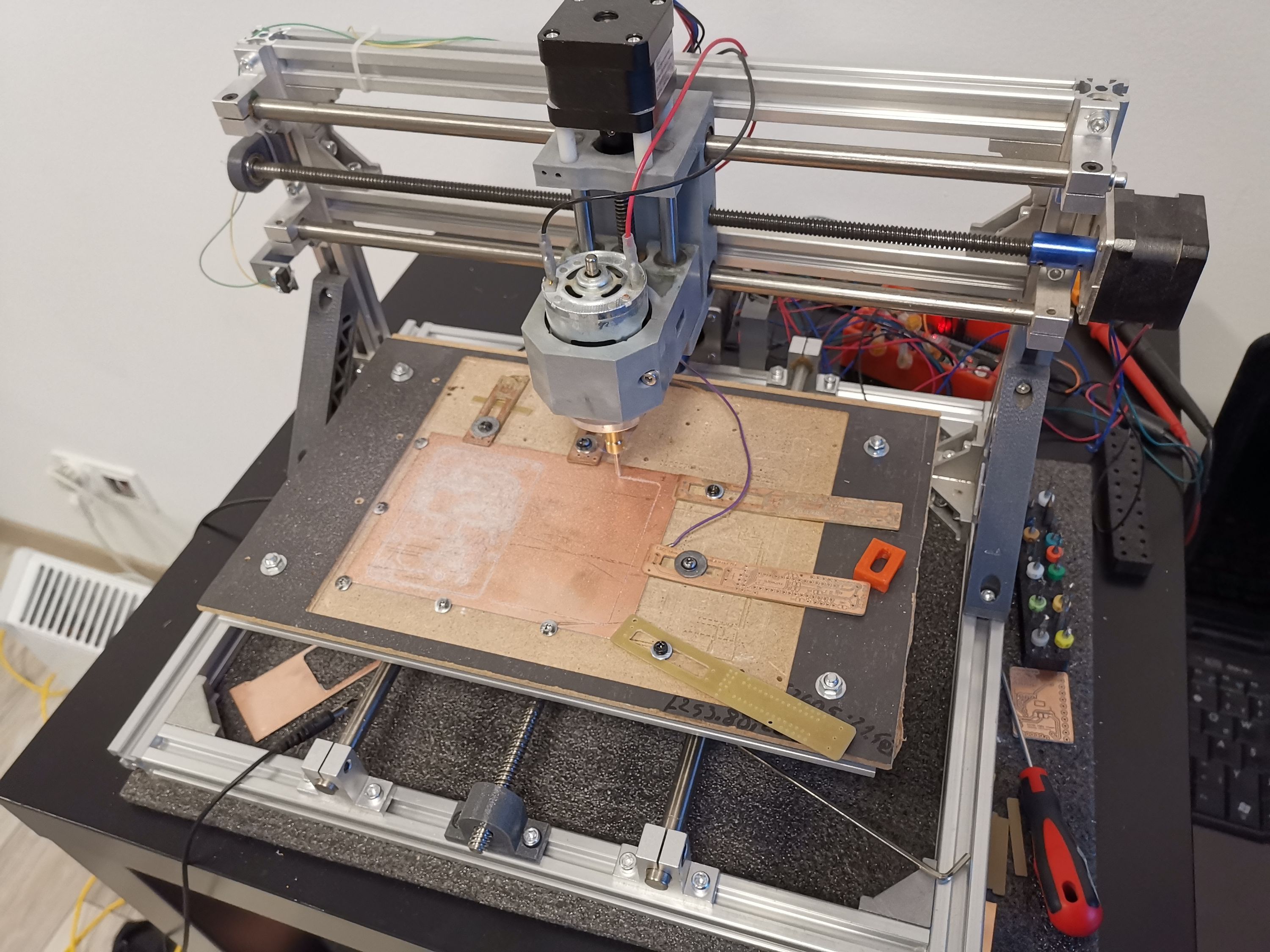
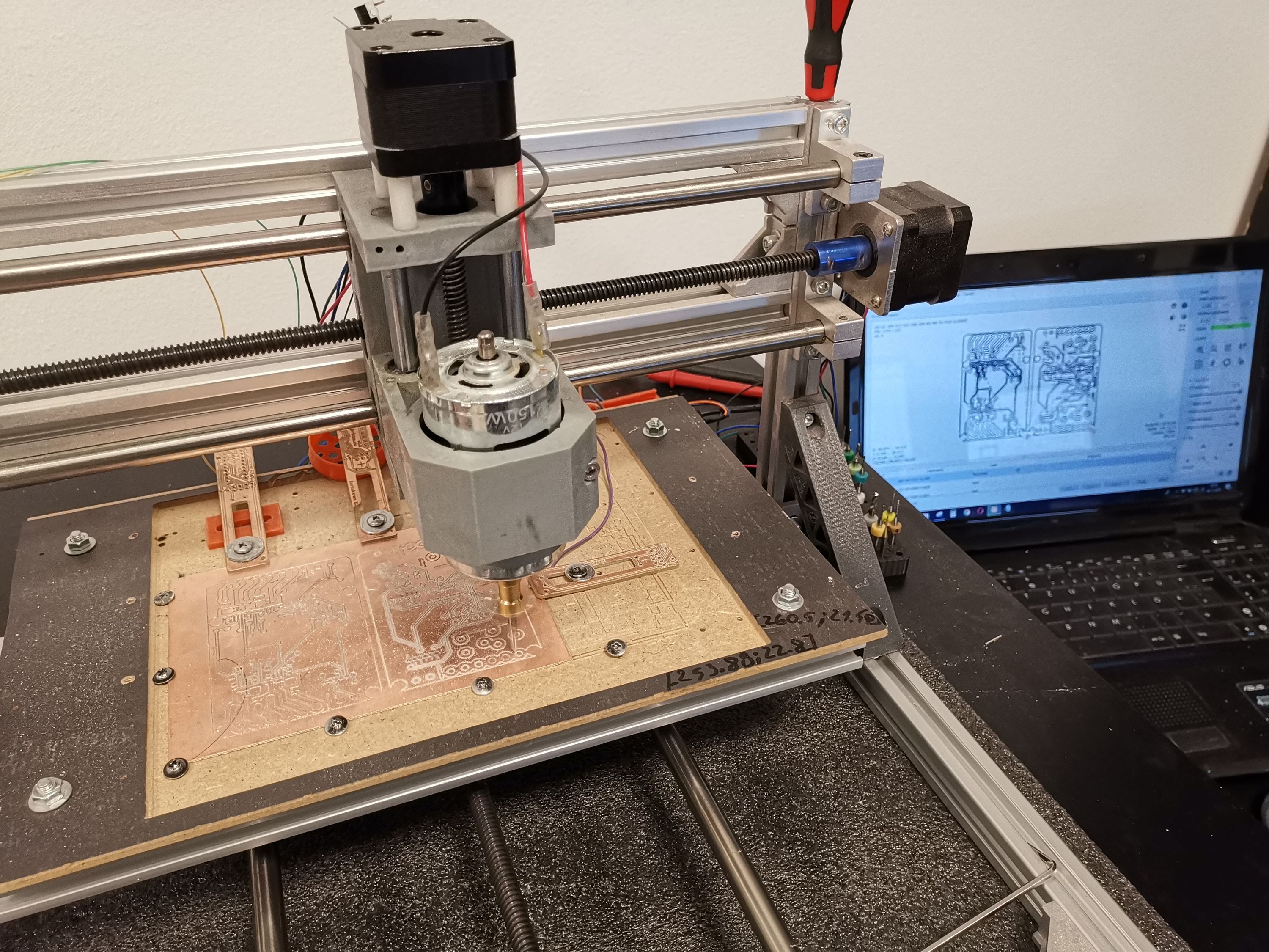
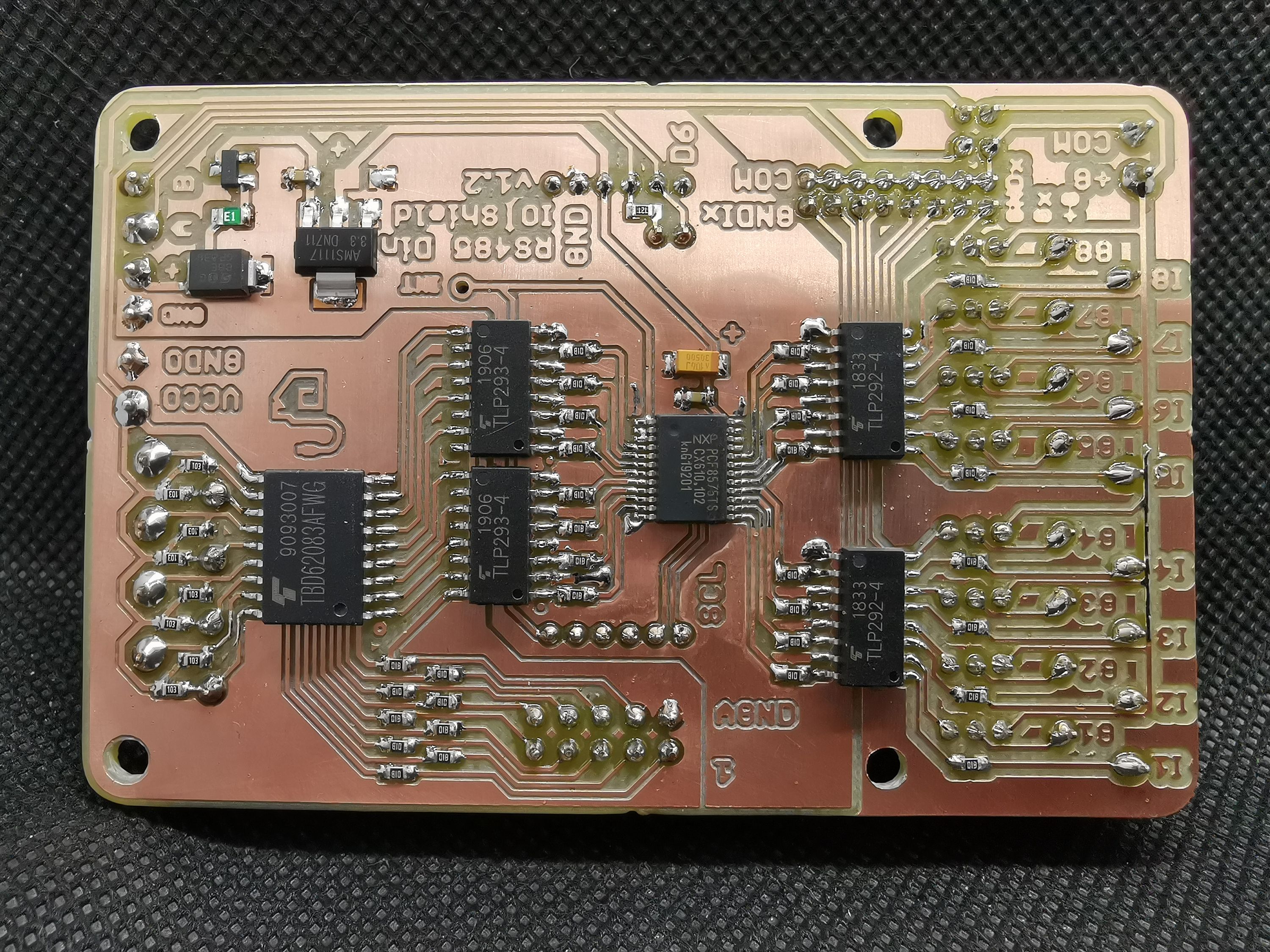
PCB Milling
Thanks to which we’ve been able to manufacture some prototypes on the spot. Though it is not possible to match the level of quality we could achieve by working with a professional PCB manufacturer, this technique has been quite helpful for us, throughout the process of developing GetWired. We used it for rapid-prototyping of less complex designs, which we were able to manufacture in a matter of hours. Thanks to PCB milling, we were able to limit our dependence on contractors in China, whose services we ended up employing only a few times.
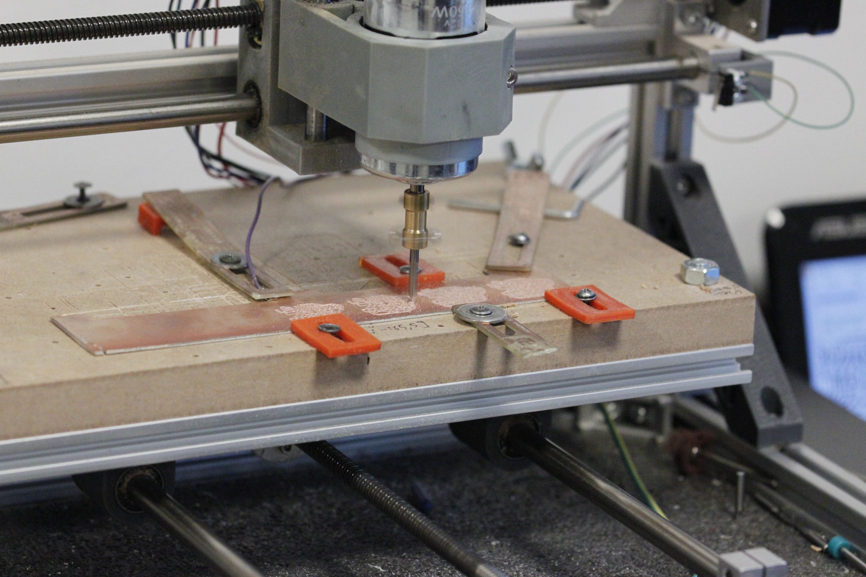
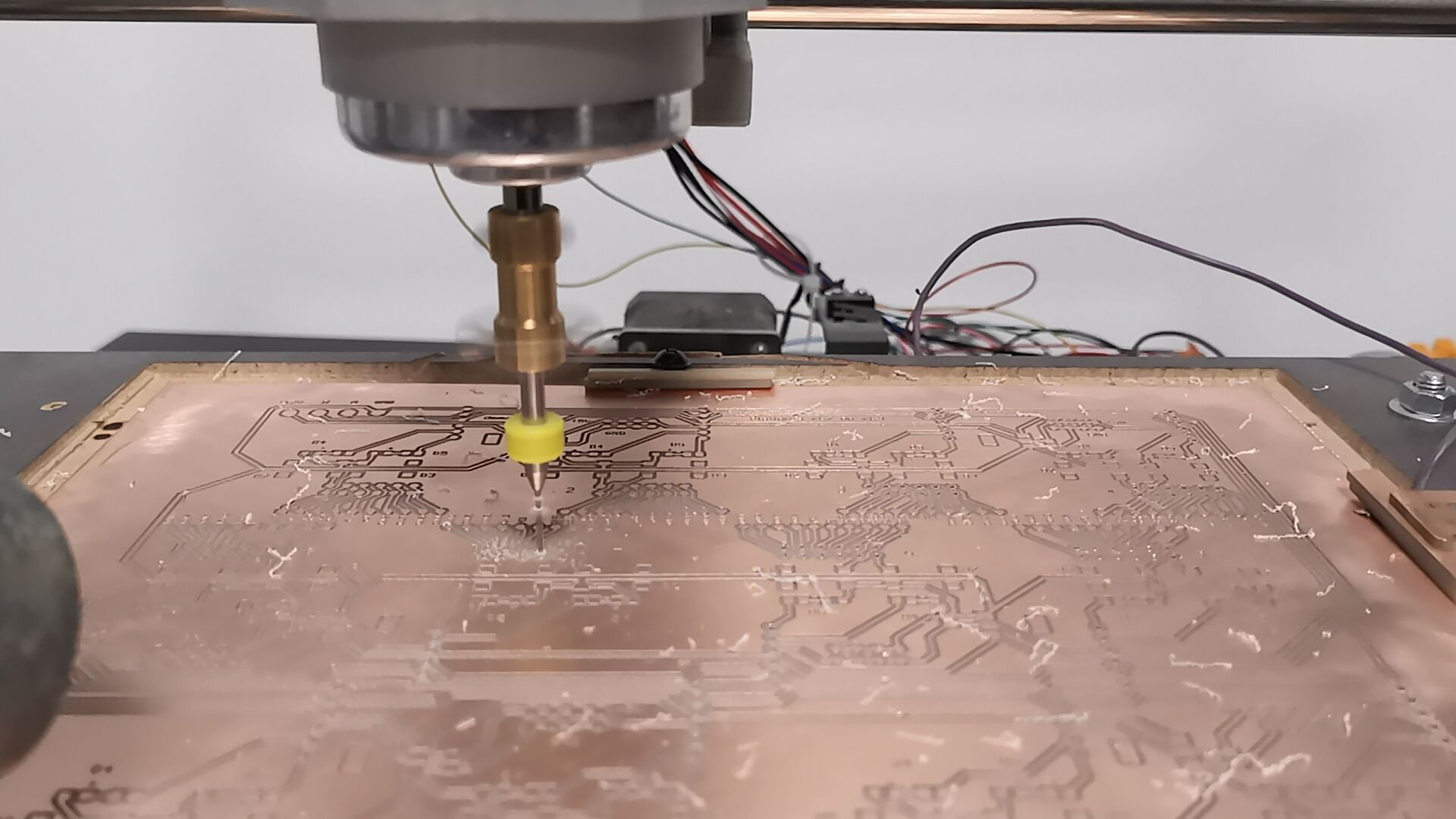
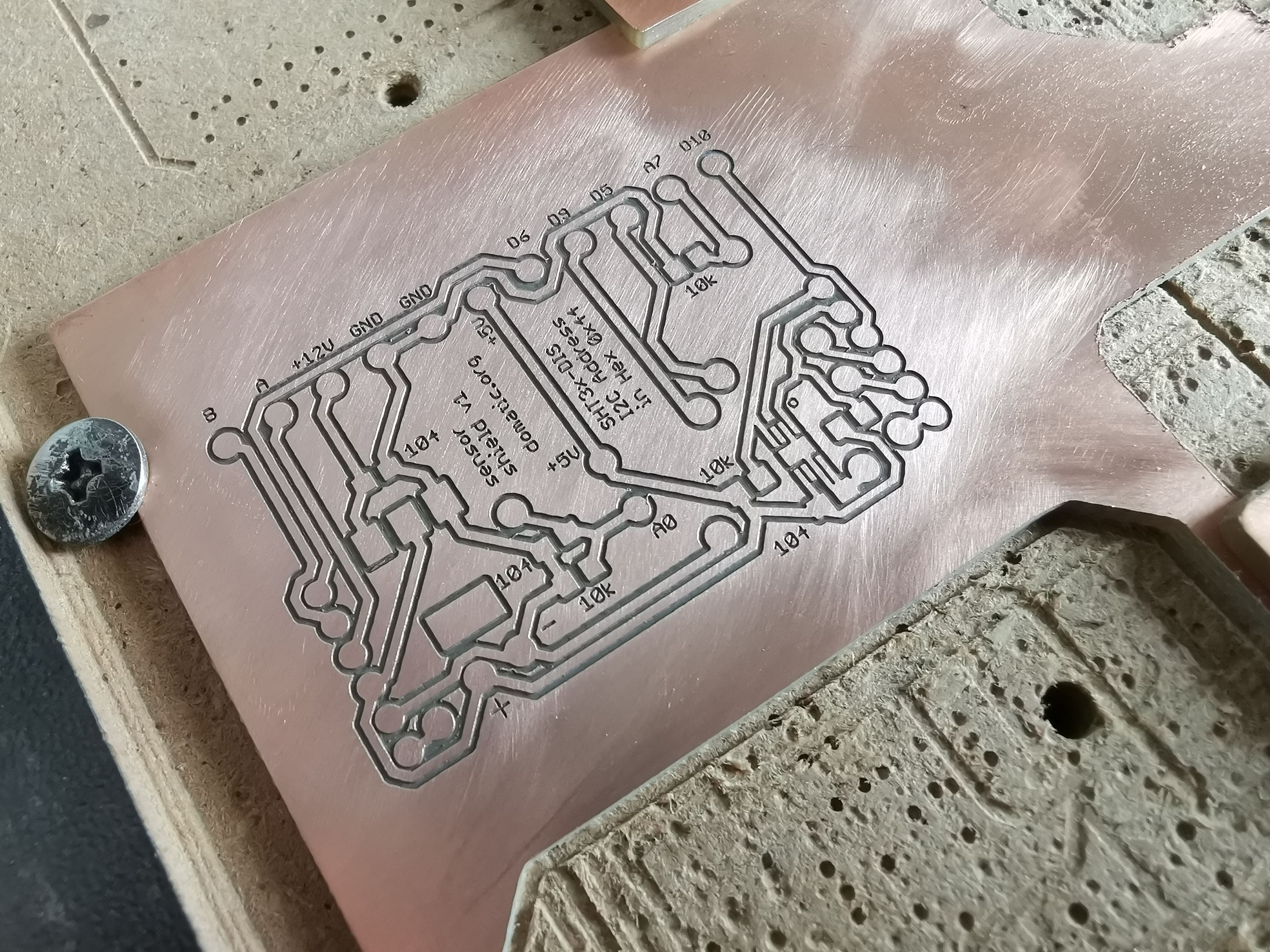
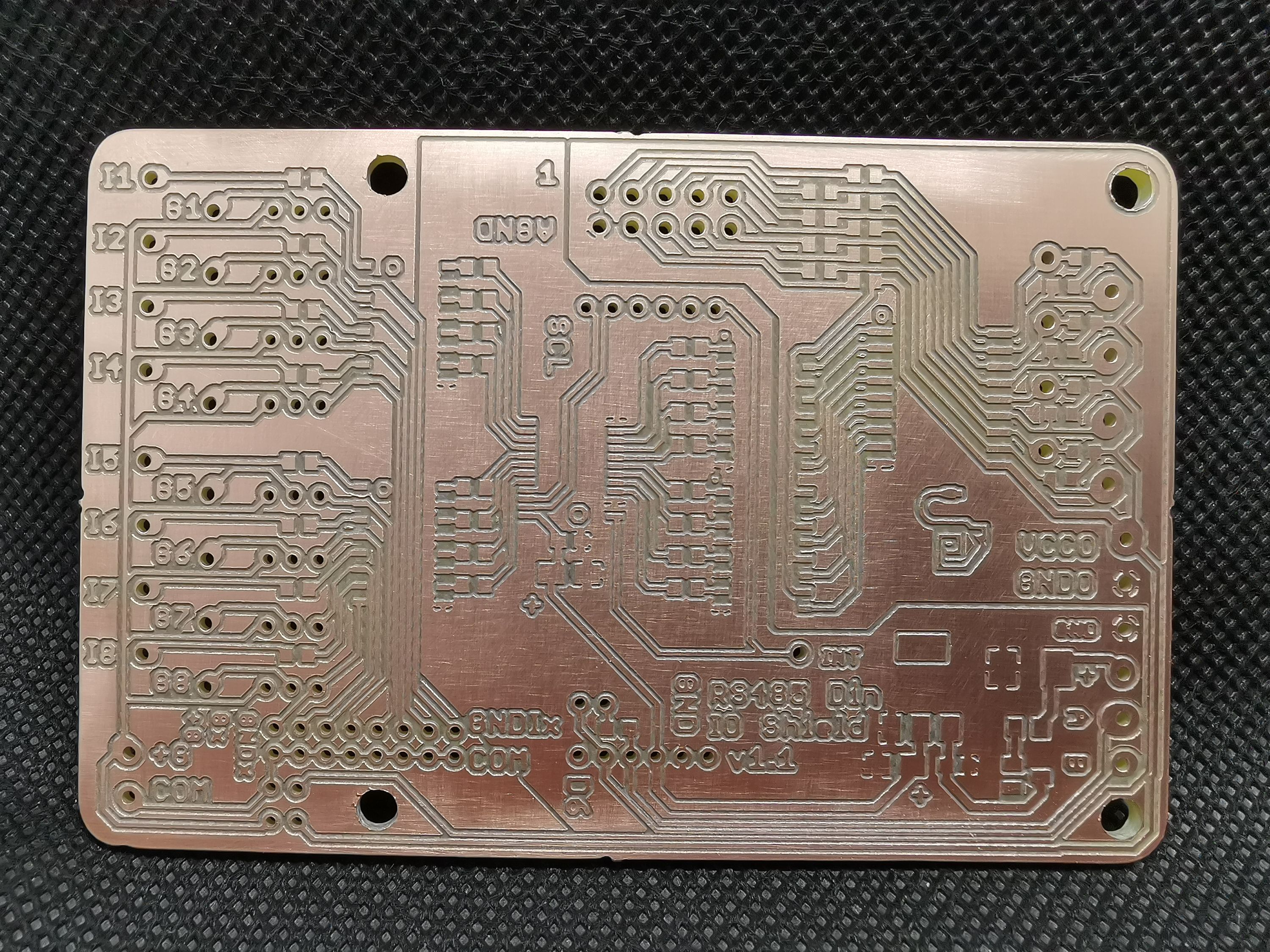
Milling Details & Photos
We own a small, desktop machine with a working area of 30 x 18 x 4.5 cm. Since PCB milling is not a very popular subject (even on the Internet), we had to develop our own methods and overcome several challenges. But, in the end, we are able to mill two-sided PCBs of up to about 26 x 17 cm. The process is quite straightforward. After the laminate has been fastened, the machine must be based to position zero, after which it will be ready to carry out the instructions specified in your G code. Photos and descriptions below.
PCB milling is not, of course, the only technique we’ve used to develop GetWired. If you’ve watched our campaign video, you’ve probably spotted a few…
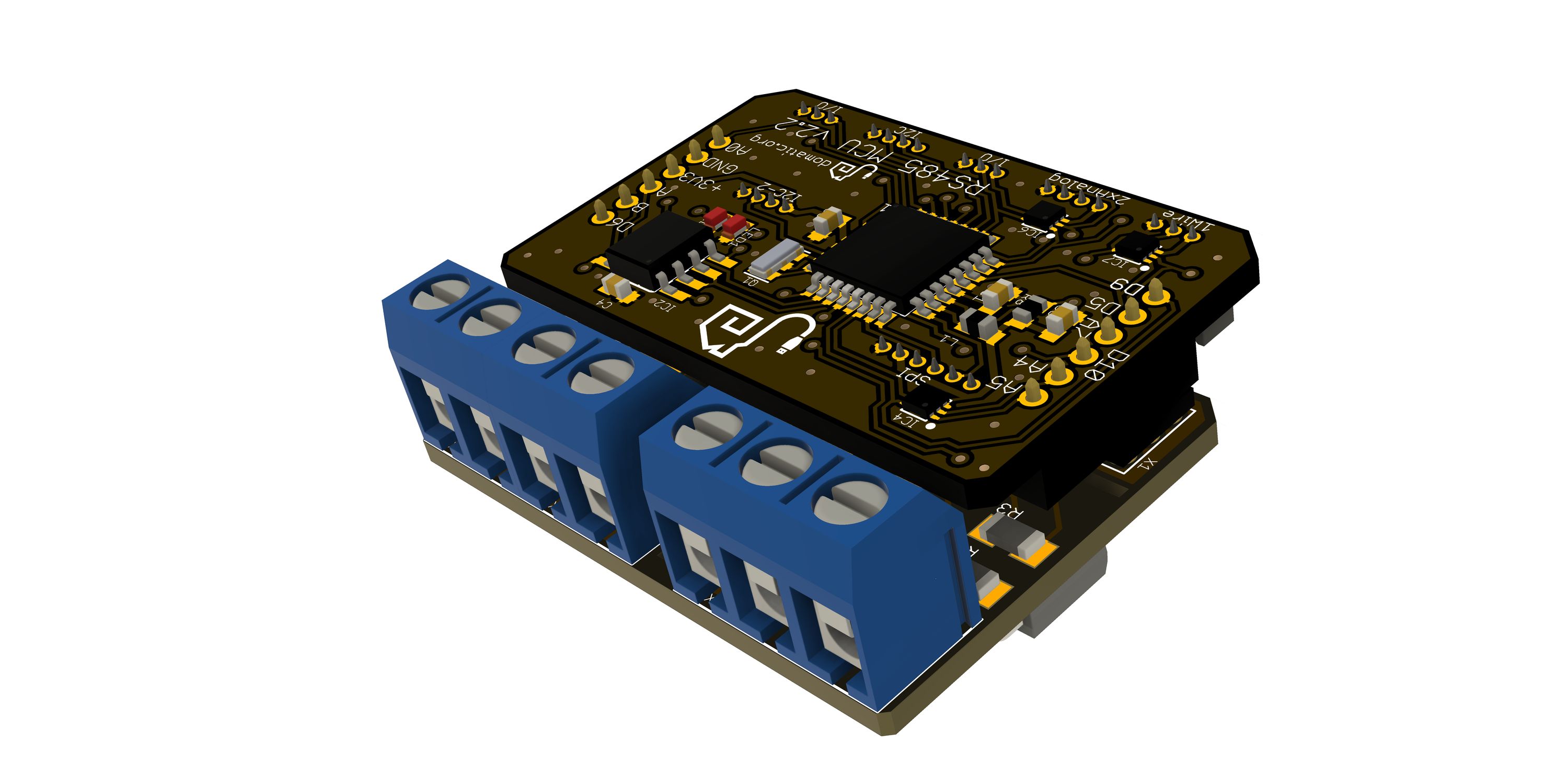
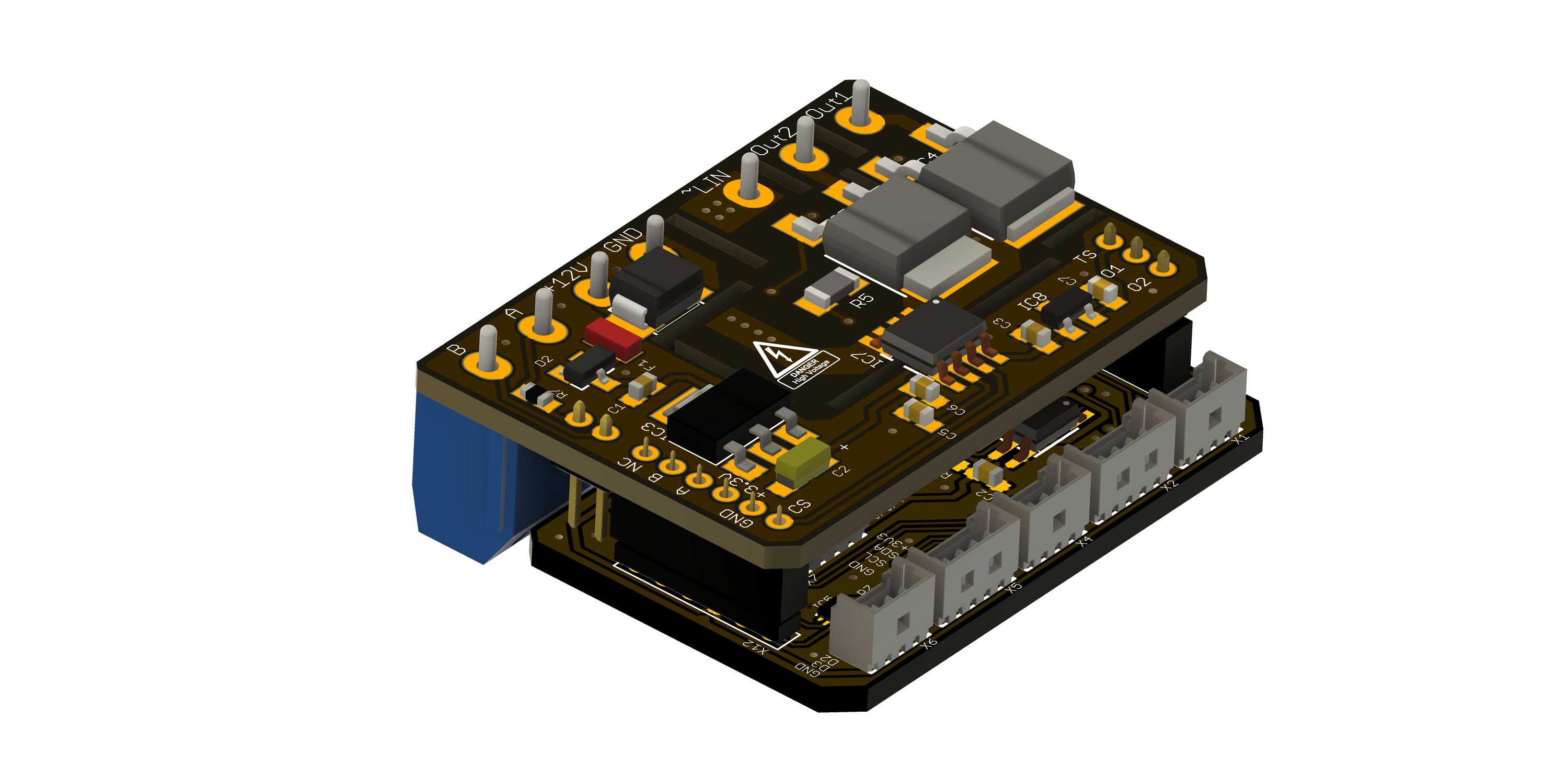
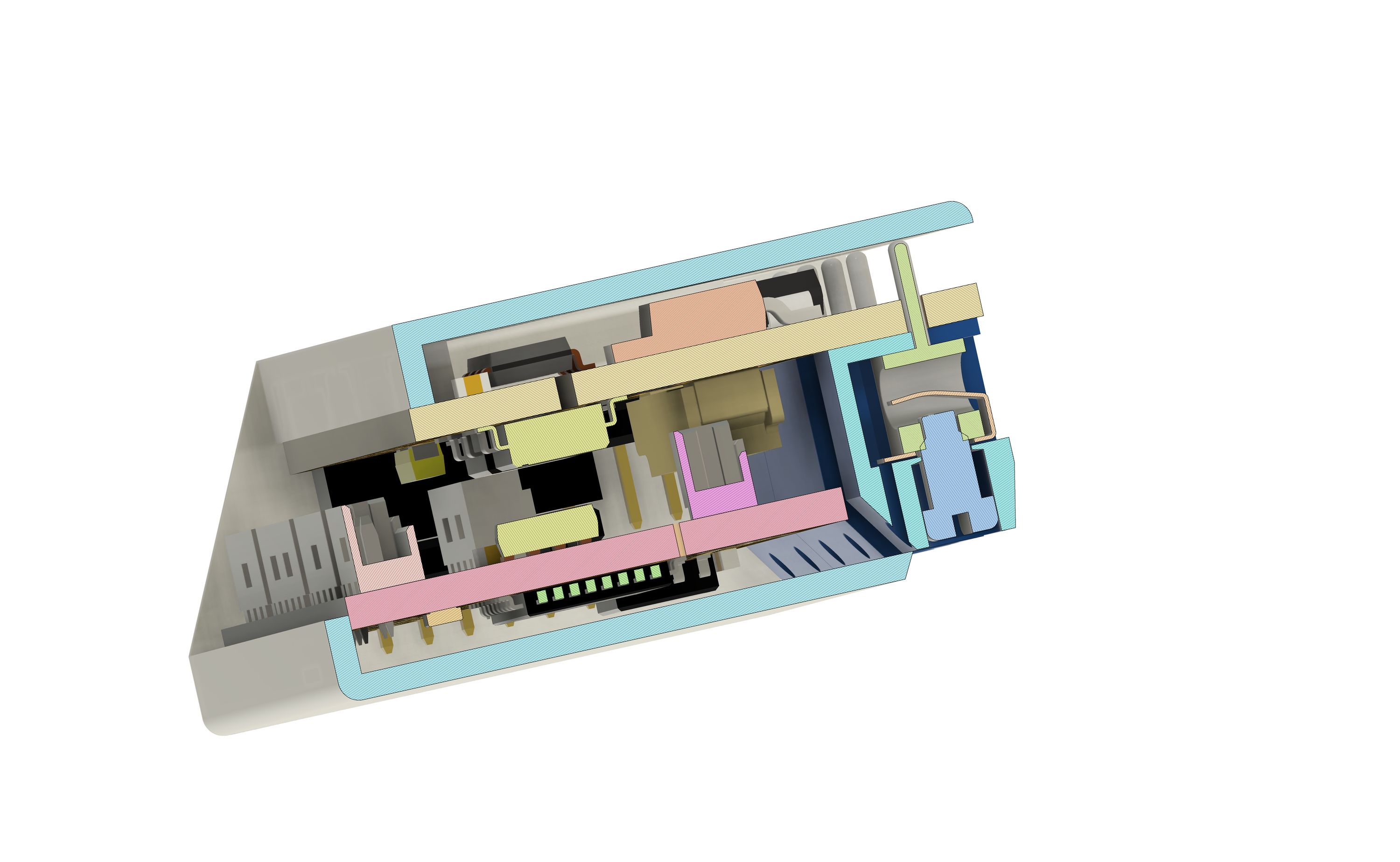
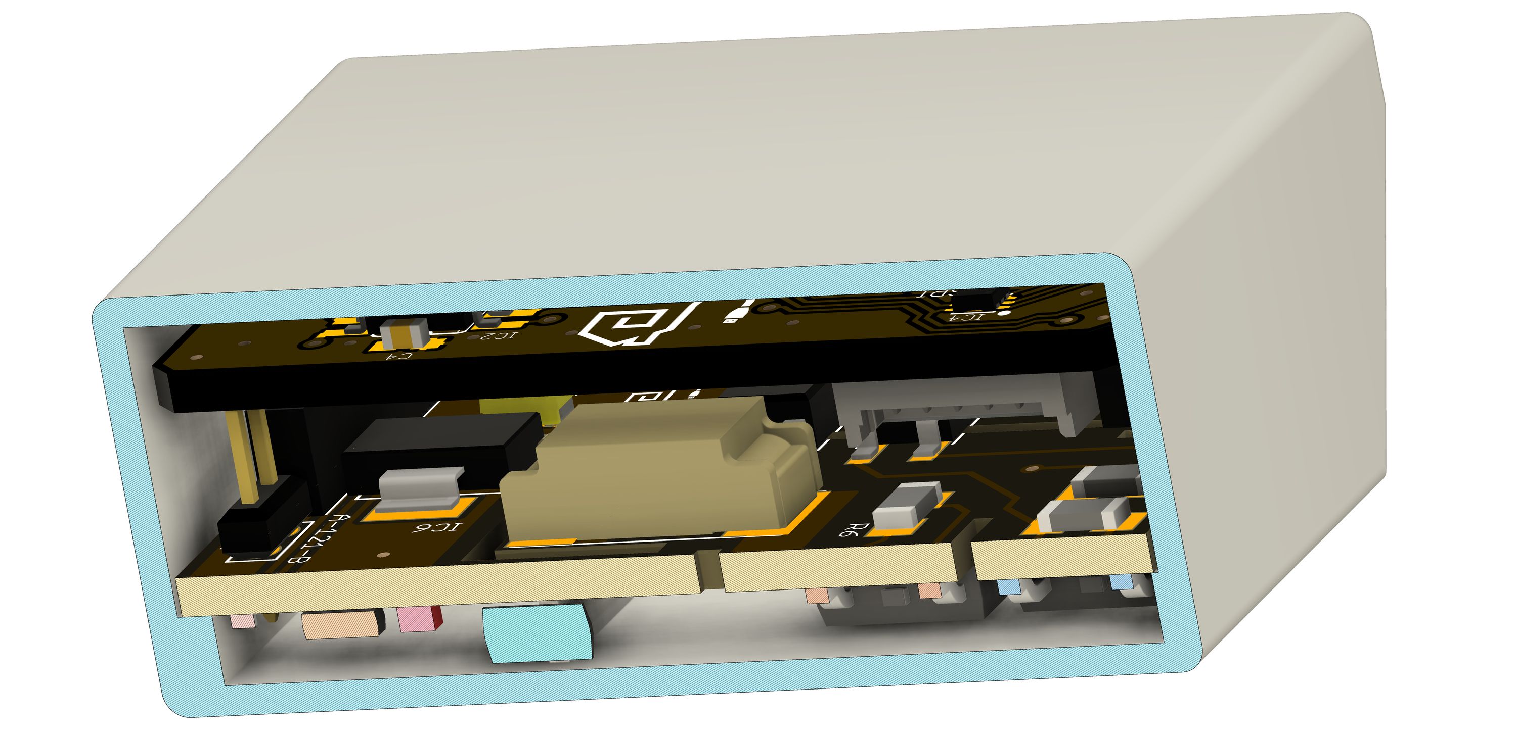
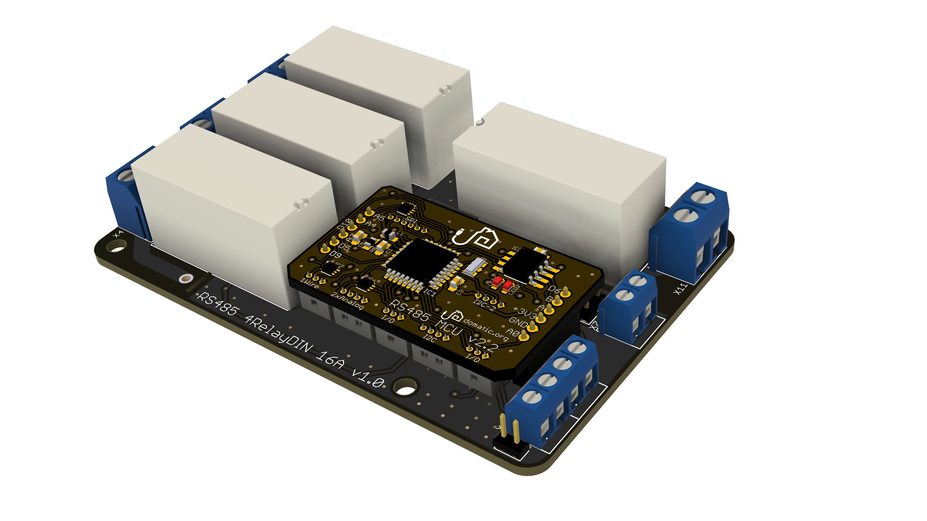
3D Visualizations
We prepared ours using Autodesk Eagle and Fusion 360, and we did so not because they look somehow impressive, but because visualizations are helpful in a very practical way when it comes time to work on certain spatially-complicated designs (which tends to be the case for GetWired modules). They’ve allowed us to verify that our MCU will fit all of our shields, which was especially important for the 2SSR Shield, given its "crowded" top layer. What’s more, our visualizations greatly facilitated the process of designing enclosures. It would have been much harder to draw the casings without them.