Project update 7 of 8
Design Deep Dive #4: Mechanical Sturdiness
by Sparsh BhonwalHi everyone,
We have some incredible news to share: USB VSense is officially funded! As we enter the final stretch of the campaign, we want to thank everyone who has joined us on this journey and, most importantly, we want to express our deepest gratitude to our backers. Your support has officially greenlit the production run.
To wrap up our technical series, we are releasing the fourth and final chapter of the Engineering Behind USB VSense story:
The "Oreo" Architecture: Turning Circuit Boards Into a Rugged, Hackable Chassis.
In our previous Design Deep Dive updates, we explored High-Voltage Resilience (#1), Ultra-High Efficiency (#2), and Thermal Stability (#3). Today, we’re shifting our focus to the structural engineering of the device. A professional field tool needs to survive being thrown in a tool bag, dropped on concrete, and plugged into ports thousands of times without succumbing to mechanical fatigue.
So, we are taking apart the Gamma revision-our final, production-ready version—to show you how we engineered a seven-PCB stack to function as a single, rigid structural block, eliminating the need for a fragile plastic shell.
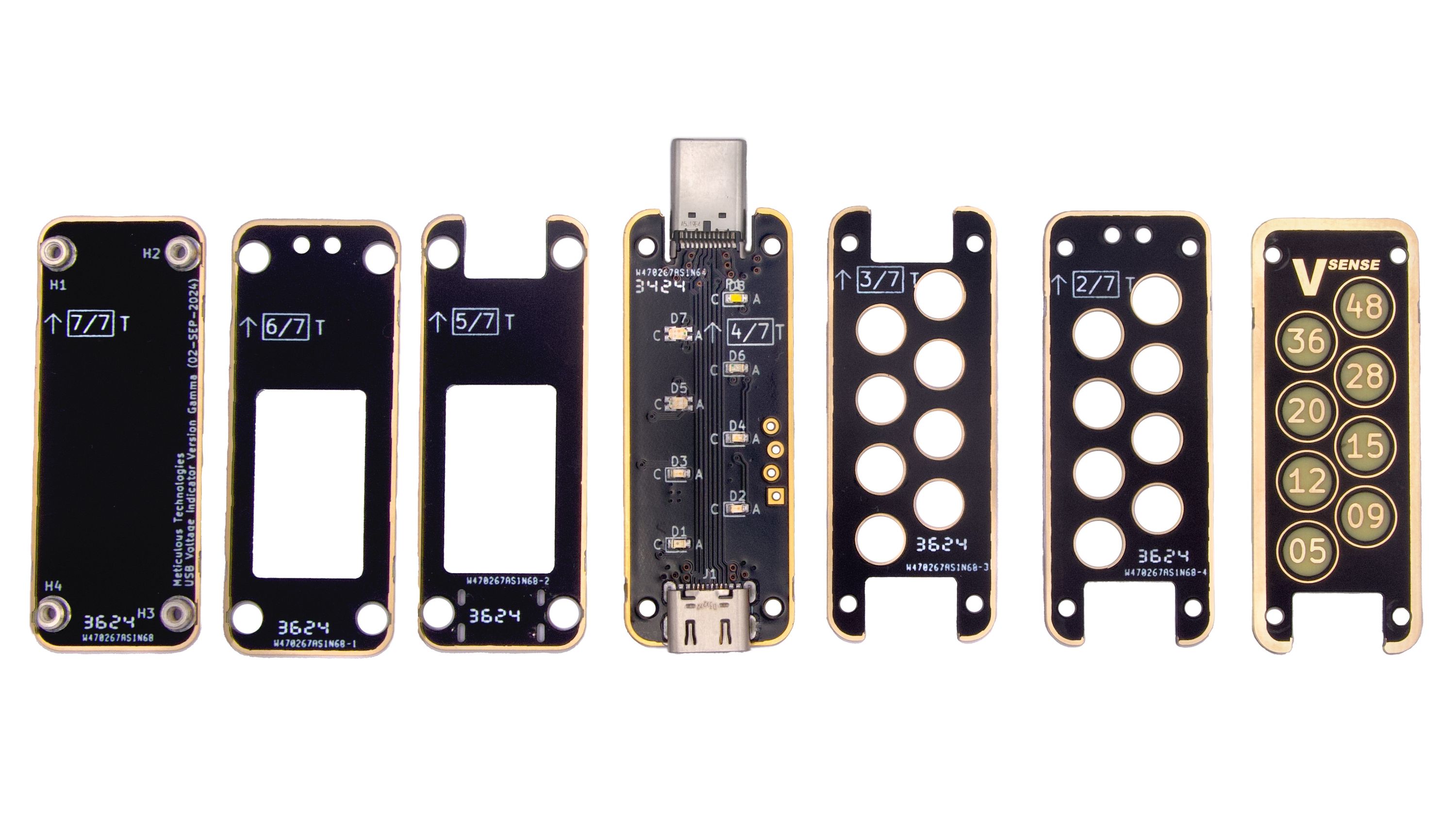
The "Oreo" Architecture: Why Stack PCBs?
Most devices use a plastic injection-molded case to hold the electronics. Instead, for USB VSense, we engineered a Stacked PCB "Oreo" Construction.
The device is composed of seven individual 0.8 mm PCBs: one central mainboard carrying the electronics, sandwiched between six structural enclosure frames. While this gives the device a distinctive, premium aesthetic, the decision was driven by three specific engineering advantages:
- Structural Rigidity: PCBs are made of FR4, a composite material consisting of woven fiberglass cloth reinforced with an epoxy resin binder. By bolting seven layers of this high-strength composite together, we create a solid "brick" that is virtually crush-proof.
- Precision Fit: Unlike injection molding, which requires "draft angles" and bulky walls, standard PCB manufacturing utilizes CNC routing. This allows us to machine zero-draft sidewalls with widths less than 500 µm. Thanks to the fiberglass reinforcement of FR4, these thin sections remain incredibly strong, allowing us to minimize the device's width without compromising structural integrity.
- Native Customizability: Because the enclosure is made of standard PCBs, users can easily "hack" the device by swapping the outer layers for custom designs.
Let’s look at how we executed each of these concepts in the final design.
Precision: Anchoring the USB-C Connector
In any dongle-style device, the USB-C plug is the primary point of failure. The technical reason is the Cantilever Effect. The plug acts as a lever arm; if you bump the device while it’s plugged in, that force creates a Mechanical Moment (Torque) at the solder joints, often cracking the connector pads.
The Seven-Layer Solution
In our earlier prototypes (five-layer stack), standard 1.6 mm frames left too much horizontal gap around the connector. For the Gamma revision, we switched to thinner, 0.8 mm layers and increased the total count to seven PCBs.
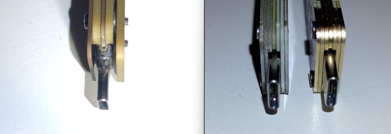
This finer stacking resolution allowed us to create a cavity that matches the JAE USB-C Plug height with less than 0.1 mm of clearance.
- Mechanical Bracing: The FR4 enclosure layers physically "hug" the metal shell of the connector, restricting it from tilting or rotating.
- Torque Absorption: By constraining rotational movement, we prevent torque from being transferred to the solder joints. Instead, external forces are absorbed directly by the rigid chassis stack.
Strength: The Steel Backbone
To hold this stack together, without using bulky external nuts that would ruin the finish, we utilize Surface-Mount Threaded Spacers (specifically the Würth Elektronik WA-SMST Series).
Think of these as steel nuts that are soldered directly onto the bottom circuit board.
- The "Invisible" Nut: These spacers are soldered onto the bottom panel like any other electronic component. Because they are permanently fused to the board, we don't need a loose nut on the outside.
- Compact Footprint: We deliberately chose M1.6 threading because the smaller diameter allows us to place these SMT spacers immediately adjacent to the USB-C connectors. This minimizes "dead space" on the PCB, significantly reducing the overall length of the device.
- Vertical Clamping: The entire stack is bolted down from the top. The screws pass through the upper layers and thread into these soldered spacers at the bottom, compressing the seven layers into a solid, rattle-free block.
Customizability: Fully Open Source Hardware
USB VSense is a fully Open Source Hardware (OSHW) project. We believe you should have total control over your tools, which is why we will be releasing the comprehensive source files for the entire device as soon as our campaign is over, and why we will be applying for OSHWA certification. This file release will include:
- Full Schematics
- PCB Design Files
- Bill of Materials (BOM)
- Assembly Instructions
- Custom Faceplate Design Files
"Fully open source" means you can easily download the faceplate template, modify it in KiCad, and order custom panels from any PCB fab. This gives you access to factory-grade finishes and modifications impossible to achieve with 3D printing:
- Functional Mods: Create a key ring attachment point by modifying one of the intermediate frame layers to include a protruding notch with a hole.
- Heavy Metal Feel: Swap standard FR4 panels for aluminum-core PCB panels to give the device a premium metallic weight and cool-to-the-touch feel.
- Unlimited Styles: Choose from any soldermask color your fab offers: purple, yellow, classic green, or matte black.
- Metallic Accents: Utilize ENIG for a luxury gold finish or HASL for a shiny silver aesthetic on exposed copper areas.
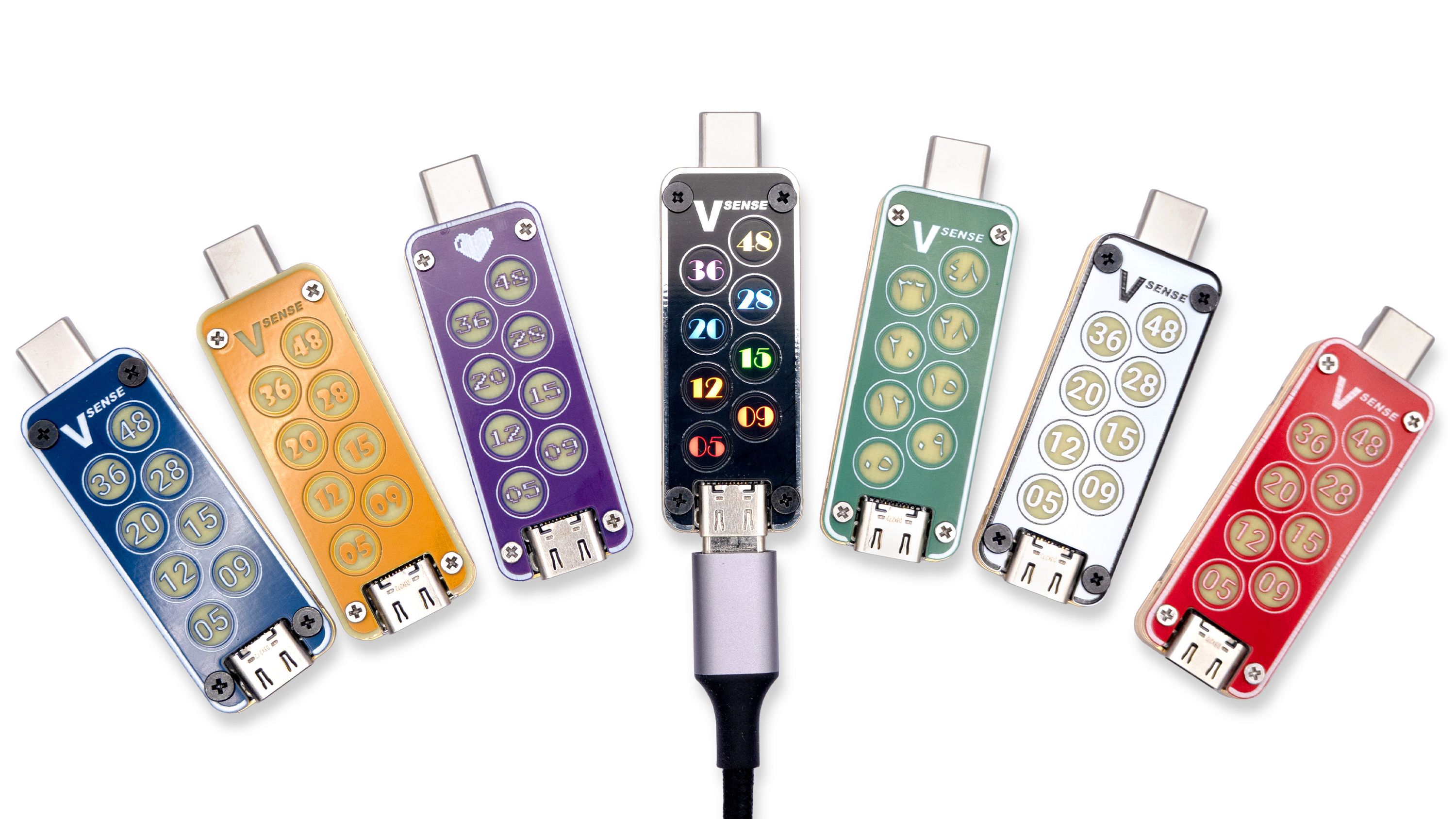
The top panel can be swapped swiftly using just four M1.6 screws, allowing you to change the face of the device in seconds.
Conclusion: Built to Last
The USB VSense wasn’t just designed to measure voltage; it was designed to be a permanent, rugged addition to your toolkit. By using SMT steel threads seven-layer precision, and the side-plated "thermal bridges" discussed in our last update, we’ve created a tool that survives the wear and tear of hard everyday use.
We hope these logs have shown that even a "simple" voltage indicator can be a masterpiece of meticulous design.
Final Call & Pricing Update
With the project now fully funded, production is guaranteed! There is still time to secure a single unit or the newly added Three Pack at the campaign price. Once the campaign concludes, the price will increase to full retail MSRP. Secure your VSense today and join the production run!
— Team Meticulous Technologies