Project update 5 of 5
Taping Out KianV - a Linux/XV6-capable RISC-V SoC
by Tim 'mithro' AnsellHi everybody!
In this update we’ll be exploring a homegrown SoC which is capable of booting Linux, µLinux and XV6. It implements the RISC-V RV32IMA ISA alongside additional extensions for more functionality.
If you’d like to explore the design, the source is available on the author’s GitHub: https://github.com/splinedrive/kianRiscV
In addition to the ASIC, a compact bring-up PCB was designed to enable hardware validation and early software development.
SoC Overview
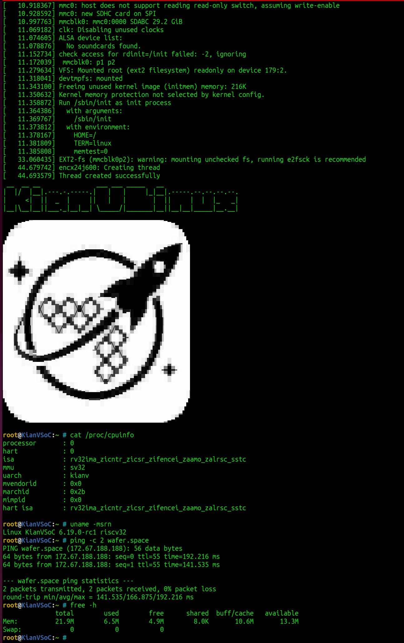
The KianV SoC is built around an RV32IMA core - that’s a 32-bit base with integer multiplication & division (M) and atomic instructions (A) extensions. In addition to those, it has support for Zicntr, Zicsr, Zifencei, SSTC and Sv32.
The Sv32 extension allows KianV to access memory - this is done using a page-based 32-bit virtual memory system, which then interacts with 32MiB of external memory through an on-board SDRAM controller.
The CPU itself includes a 2-way set-associative instruction cache, a direct-mapped data cache, and 4-way associative instruction and data TLBs, sufficient for MMU-based operating systems.
Furthermore, KianV integrates a minimal peripheral set connected via an internal system bus. The peripherals are listed below:
- SDRAM controller (interacting with 32 MiB external memory)
- UART
- 2× SPI interfaces
- GPIO
- NOR flash controller
With these peripherals, the system is capable of booting from an external SD card and accessing networked resources via an SPI-based Ethernet connection. A system like this may find uses in a variety of situations: industrial, IoT or educational.

Pinout
The pinout is designed around a strict 58 external IO signal limit, all divided between the peripherals mentioned beforehand. The wafer.space template provides access to 74 pads, however these also include power and ground connections.
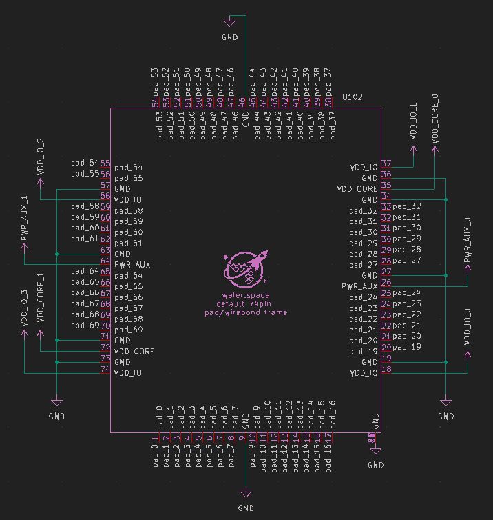
| Interface | Signals | Dir | Description |
|---|---|---|---|
| UART | RX, TX | I/O | Serial console |
| SPI0 | CS#, SCLK, MOSI, MISO | I/O | SD card |
| SPI1 | CS#, SCLK, MOSI, MISO | I/O | Ethernet |
| Flash | CS#, SCLK, MOSI, MISO | I/O | SPI NOR flash |
| SDRAM | CLK, CKE | Out | Clocking |
ADDR[12:0] | Out | Address bus | |
BA[1:0] | Out | Bank select | |
DQ[15:0] | I/O | Data bus | |
DQM[1:0] | Out | Byte mask | |
CS#, RAS#, CAS#, WE# | Out | Control signals | |
| GPIO | GPIO0 | I/O | General-purpose IO |
Signals are grouped by function; directions are given from the SoC perspective.
Design Philosophy
The RISC-V processor in this SoC is a multi-cycle RV32 core, optimized for area. The architecture was validated prior to taping out on FPGA platforms, where SV32-capable mainline Linux and network connectivity were demonstrated.
Likewise, a µLinux (no-MMU) version of the KianV SoC was fabricated on multiple shuttles run by Tiny Tapeout, providing silicon validation of the core and peripheral subsystems. You can view these submissions online on the Tiny Tapeout website: TTSky25a, TTIHP25b, TTSky25b and TTIHP26a.
KianV is also mentioned in a FOSSi Foundation article and referenced in an IEEE Solid-State Circuits Magazine publication.
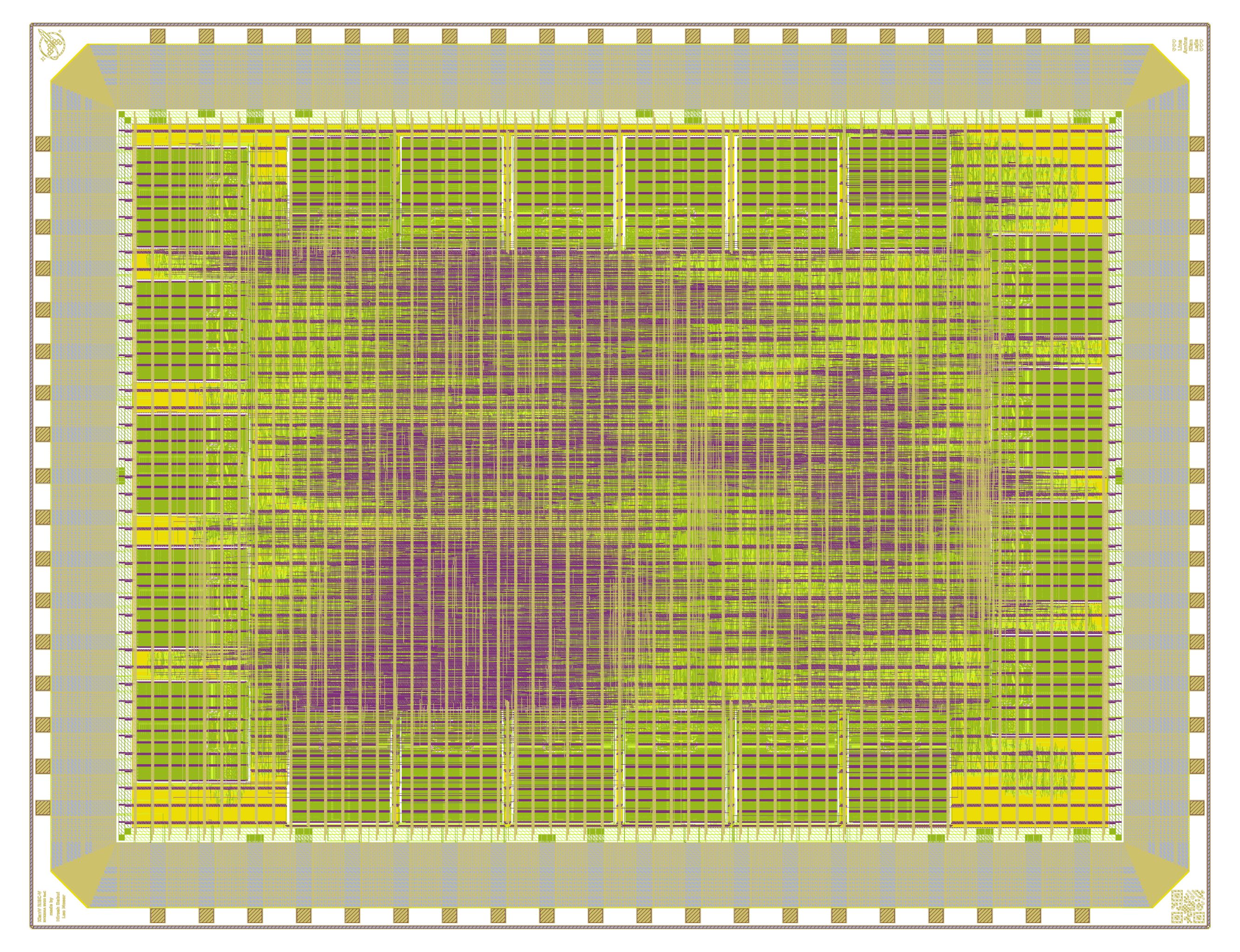
Design Flow
KianV was brought to life using LibreLane and the wafer.space GF180MCU project template, which was then submitted to Run 1, and manufactured using the GlobalFoundries 180 nm PDK.
The flow provided by the project template covers everything you’d need to produce and successfully tapeout a design. It contains software for RTL synthesis, floorplanning, place-and-route, clock tree synthesis and physical verification using known open-source tools.
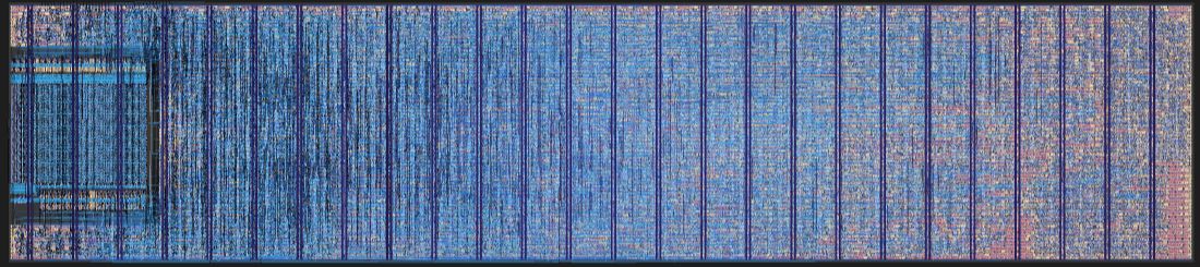
Implementation Results
Linux was booted in a gate-level simulation which painstakingly ran for an entire month before reaching the login prompt. This was using the mainline 6.19 version of the Linux kernel, and was validated against a Micron SDRAM simulation model driven by the author’s SDRAM controller.
Run 1 silicon is being shipped as we speak, so why not join our Discord or Matrix channels to see some silicon validation?
KianV was taped out onto a full-sized die (20.1 mm²), with an approximate core utilization of 65% and an estimated ~13 mW of power consumption.
Design Validation PCB
As mentioned in the introduction, a small bring-up PCB was designed to support validation and software bring-up.
The board provides a number of supporting components, such as the 32 MiB of SDRAM, an SPI-based Ethernet connection, SPI flash, SPI SD card interface, UART access and a power supply.
This PCB is available to view on GitHub too: https://github.com/splinedrive/gf180mcu-kianv-pcb
Software Status
KianV uses a custom bootloader, followed by OpenSBI, and then boots the Linux kernel. Only minimal driver adaptations were required to boot mainline Linux with Sv32 MMU support on the SoC.
In addition to Linux, the system also runs µLinux and XV6 on the same hardware platform.
Acknowledgments
- Andrew Wingate - Board design review (wafer.space)
- Christian Stredicke - Voida PBX
- Goran Maholvic - Board design support and SDRAM routing
- Leo Moser - ASIC flow and PDK support (wafer.space)
- Marcelo Samsoniuk - For the technical and personal exchange over the past few years (DarkRiscV)
- Matt Venn - Tiny Tapeout
- Sylvain Munaut - Tiny Tapeout
- Tim Ansell - Founder of wafer.space
- Uri Shaked - Tiny Tapeout
Additional Resources
- KianV SoC Design: https://github.com/splinedrive/gf180mcu-kianv-rv32ima-sv32
- Bring-up PCB Design: https://github.com/splinedrive/gf180mcu-kianv-pcb
- Carl Karsten - Online access to FPGAs (with ASICs coming soon): https://ps1.fpgas.online/
- Matt Venn - RISC-V/Open Source Silicon Stream updates: https://www.linkedin.com/posts/matt-venn_riscv-opensourcesiliconstream-activity-7290765655132274690-Hfgw
- Matt Venn - Tiny Tapeout ASIC/Open Source development: https://www.linkedin.com/posts/matt-venn_asic-opensource-riscv-activity-7279556029233704960-d5ZO
- Uri Shaked - Tiny Tapeout project update: https://www.linkedin.com/feed/update/urn:li:activity:7312742011252490240/
- Zero to ASIC Course 2024 Highlights: https://www.zerotoasiccourse.com/post/year_update_2024/#2024-highlights