wafer.space GF180MCU Run 2
Fabricate 1,000 chips of your own design
Back this project to help bring it into existence.
Funding ends on Jun 30, 2026 at 04:59 AM PDT.
Back this project to help bring it into existence.
Funding ends on Jun 30, 2026 at 04:59 AM PDT.
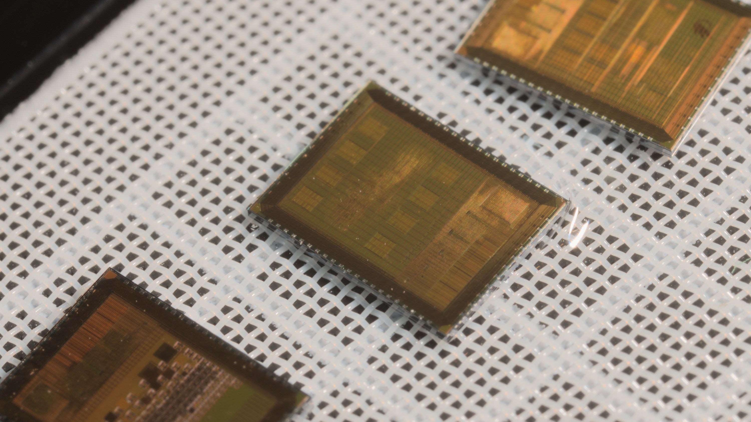
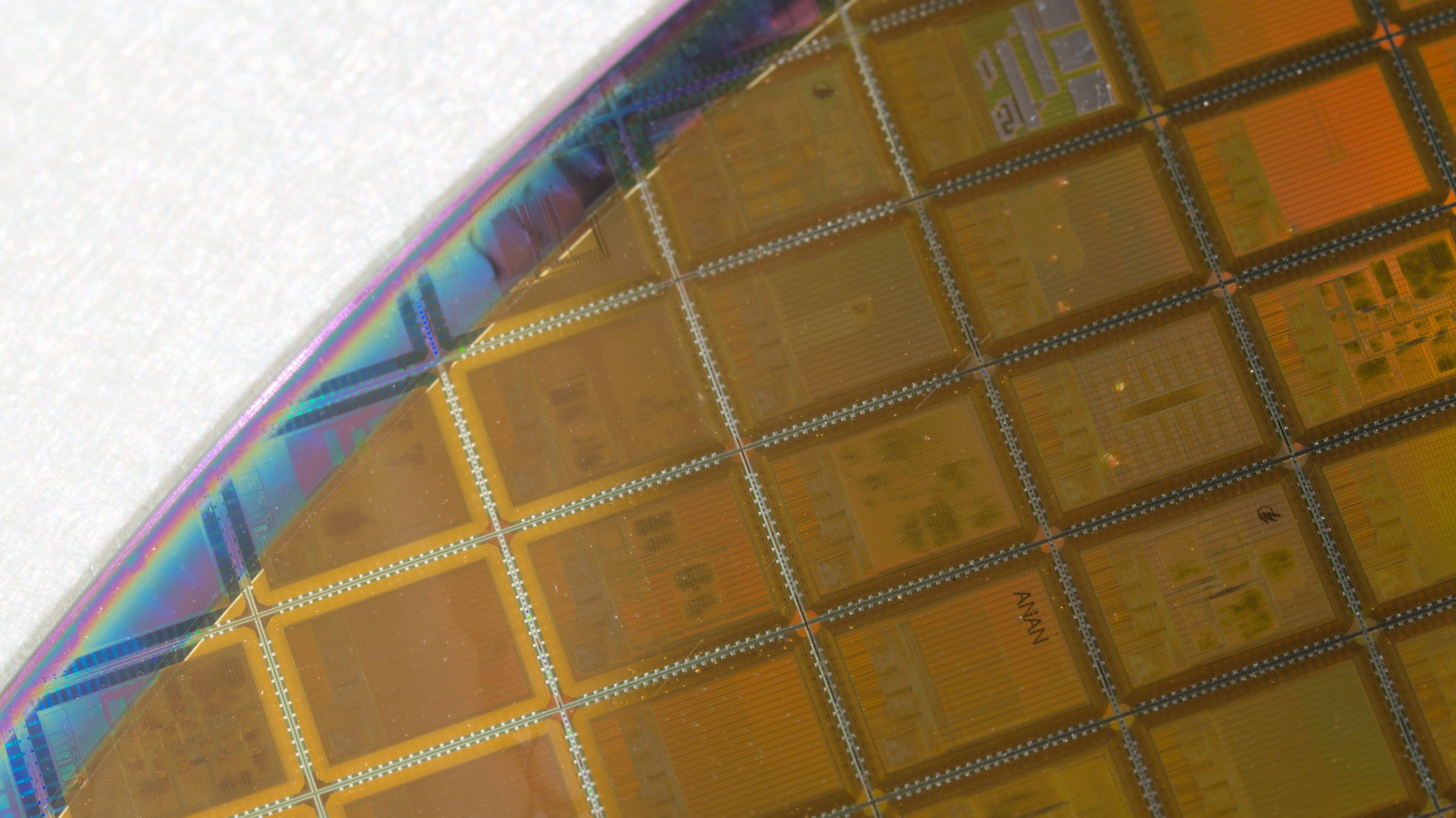
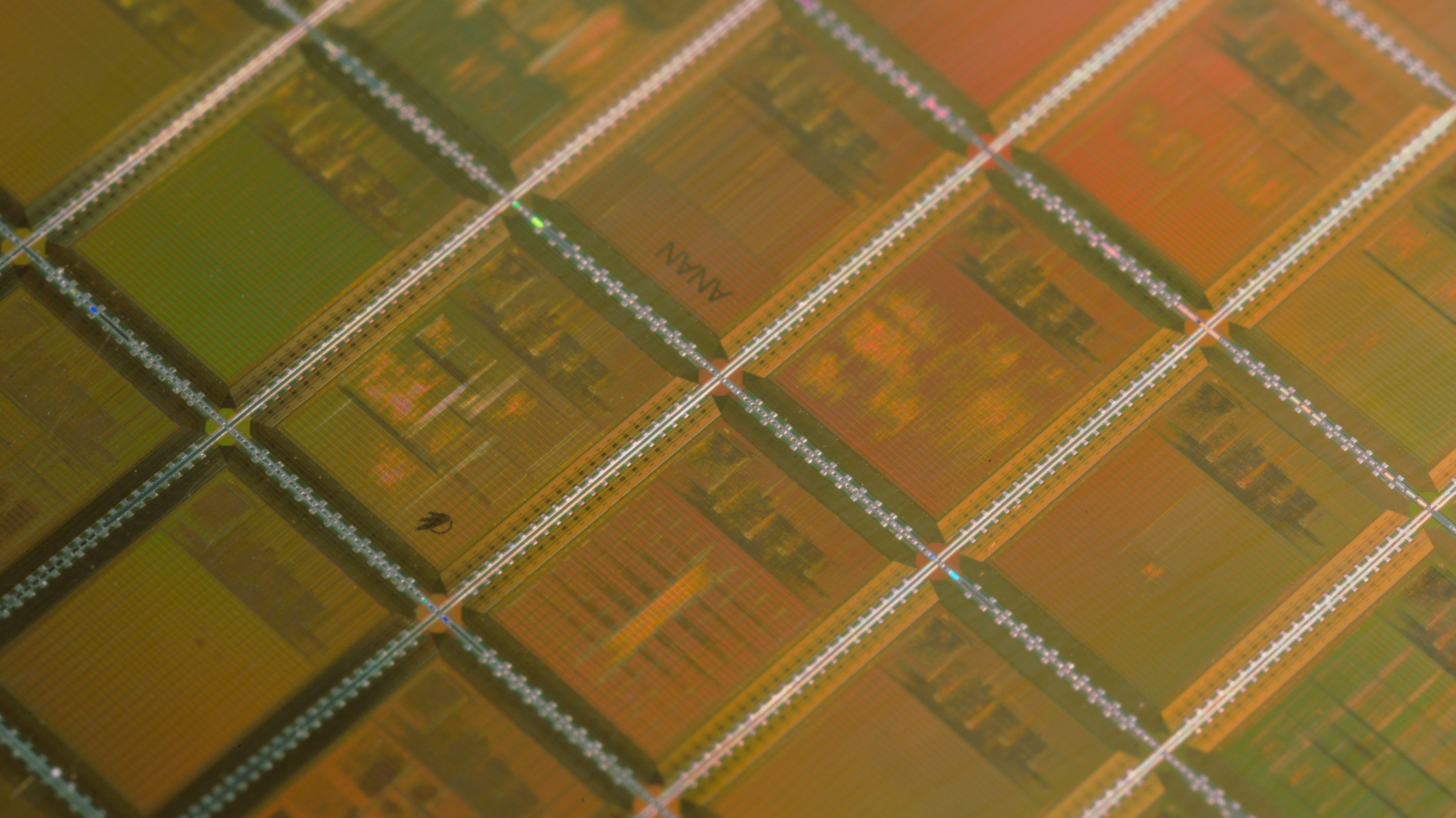
Get 1,000 custom silicon dies from as low as $4 per die with early bird pricing. wafer.space‘s second production run on GlobalFoundries’ GF180MCU 180 nm mixed-signal process is open for purchases. You design your chip, we handle fabrication, dicing, and delivery. No gatekeeping, no opaque quotes, no five-figure NRE.
Run 2 builds on Run 1, where many designs were submitted by universities, startups, hobbyists, and established engineers from around the world. New for Run 2: half-width and half-height slot options starting at $4,000, stricter DRC checking, and an improved submission platform.
Orders were painful: opaque quotes, setup fees, big MOQs, long waits, and DIY panelization. Then pooling services like OSH Park fixed it with predictable pricing, frequent runs, and no-nonsense logistics. wafer.space brings that shift to silicon.
Run 2 offers three slot sizes. All sizes use the same GF180MCU process, the same padframe infrastructure, and the same submission platform. Every slot includes 1,000 dies.
| 1x1 (Full) | 0.5x1 (Half Width) | 1x0.5 (Half Height) | |
|---|---|---|---|
| Die Size | 3.93 mm x 5.12 mm | 1.94 mm x 5.12 mm | 3.93 mm x 2.53 mm |
| Die Area | 20.12 mm2 | 9.93 mm2 | 9.94 mm2 |
| Usable Silicon | 19.65 mm2 | 9.57 mm2 | 9.61 mm2 |
| Core Area | 12.92 mm2 | 4.46 mm2 | 5.02 mm2 |
| Default I/O Count | 56 | 56 | 56 |
| Default Total Pads | 72 | 72 | 72 |
| Early Bird Price | $7,000 ($7/die) | $4,000 ($4/die) | $4,000 ($4/die) |
| Standard Price | $7,500 ($7.50/die) | $4,500 ($4.50/die) | $4,500 ($4.50/die) |
Usable silicon is the die area minus the seal ring (~26 um each side). This is the area available when using a custom pad ring or no pad ring. Core area is the area inside the default pad ring.
Early bird pricing is available through 30 April 2026.
For detailed slot specifications including padframe layouts and design constraints, see the slot size documentation.
Choosing a slot size: The 0.5x1 (half width) gives a tall, narrow die, ideal for I/O-heavy designs where signals concentrate along the long edges. The 1x0.5 (half height) gives a wide, short die, ideal for designs that benefit from a wider core. The 1x1 (full) provides maximum area for complex SoCs and mixed-signal designs. All three sizes share the same 56 I/O and 72 total pad configuration.
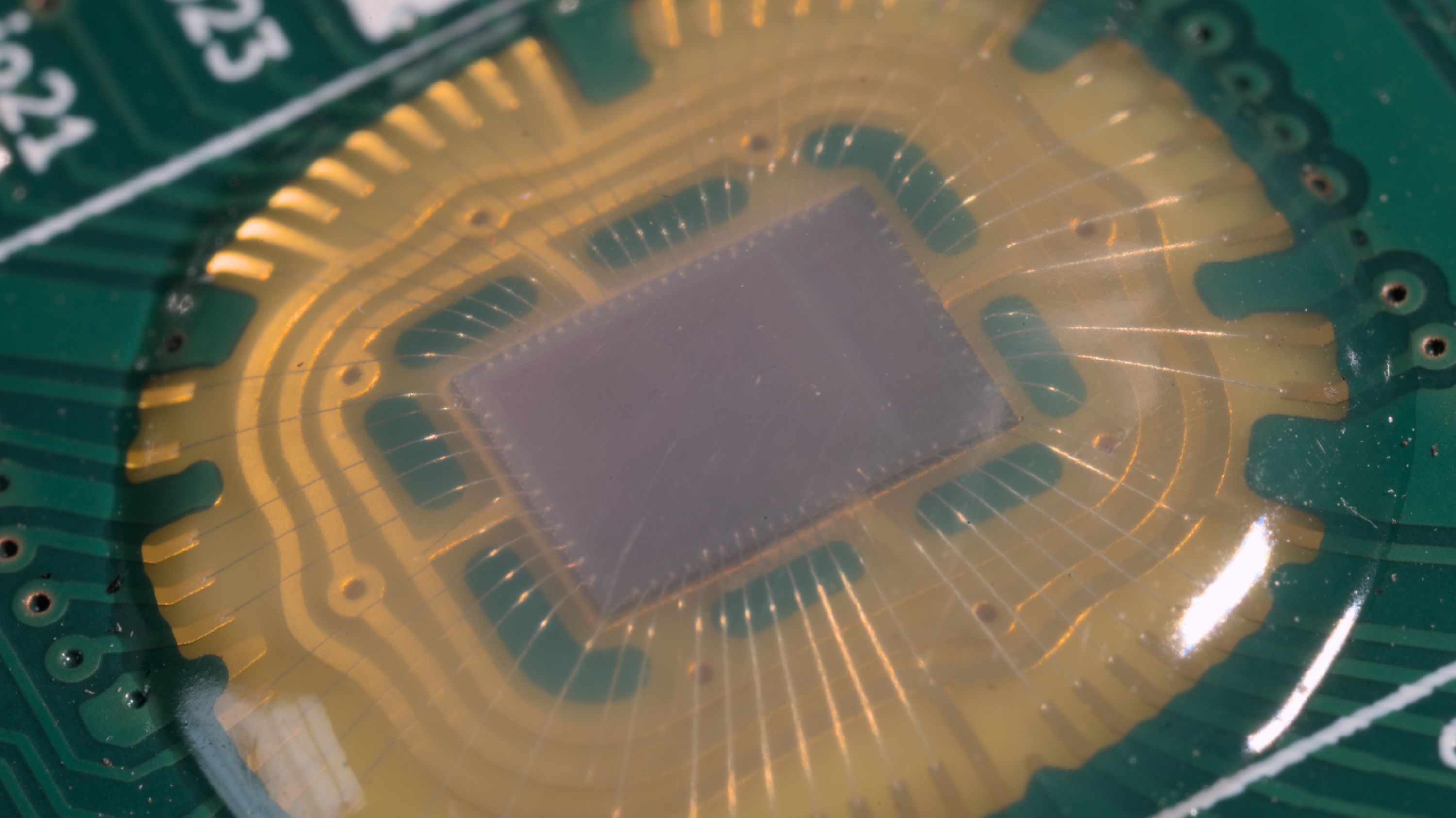
Receive your dies wire-bonded onto small PCBs, ready for testing and integration.
Add-on to any slot purchase.
Take home a complete 200 mm wafer containing all Run 2 designs.
Requires slot purchase.
GF180MCU Run 1 closed in November 2025 with a full reticle of many designs from universities, startups, hobbyists, and established engineers around the world. Silicon is currently in fabrication at GlobalFoundries. 29 of those designs are publicly available at github.com/wafer-space/ws-run1.
Run 2 incorporates everything we learned from that first production cycle: better DRC coverage, more slot size options, and a smoother submission workflow.
The gf180mcu-project-template provides a ready-to-use starting point with LibreLane configuration, a Nix-based development environment, cocotb testbenches, and example designs. Clone it, drop in your Verilog, and run make librelane to go from RTL to GDS.
| Date | Milestone |
|---|---|
| 1 March 2026 | Campaign opens on Crowd Supply. |
| 30 April 2026 | Early bird pricing deadline. |
| 30 June 2026 | Final deadline to purchase slots. |
| 14 July 2026 | Final deadline to submit clean GDS. |
| Early Q4 2026 | Bare dies and packaged parts shipped to customers. |
Purchase your slot today and lock in early bird pricing before 30 April 2026.
Professional design services are available from independent consultants experienced with the GF180MCU process. Options include full custom design, verification help, or guidance on a first tapeout. See the design help page for details.
No. The PDK is open; your design can be open or closed. In Run 1, most Run 1 designs chose to be open-source, but that is entirely up to you.
Start with your design’s area requirements. If your layout fits comfortably in the core area of a smaller slot, use the smaller slot and save money. If you need the full 12.92 mm2 of core area, go with the 1x1. The slot size documentation has detailed padframe layouts and constraints for each size.
As a rough guide:
Yes. You own the full die area of your slot. You can place multiple test chips, multiple macros, or any combination you want within your allocated space. Several Run 1 participants did exactly this.
Yes. The 29 public Run 1 designs at github.com/wafer-space/ws-run1 are available for reference. Note that slot dimensions have changed slightly for Run 2, so you will need to adjust padframe configurations. The project template is the best starting point for new designs.
No, but the community has created example pad rings and reviews of common pitfalls. The gf180mcu-project-template includes a default padframe configuration, and there are 29 public Run 1 designs you can use as references.
All three slot sizes support up to 56 I/O with 72 pads total. The actual number you use depends on your pad pitch and die edge budget.
The Run 2 precheck system has broader DRC rule coverage and catches more edge cases that were missed in Run 1. This benefits everyone: designs that pass the stricter checks are more likely to work correctly in silicon. Run the precheck locally before submitting to catch issues early.
Fabricated on GF180MCU at GlobalFoundries in Singapore. Dicing and logistics via qualified partners. Final shipping from Singapore or our fulfillment partner.
You are responsible for your own design, but you are not alone. The wafer.space community is active and helpful.
Ready to get started? Purchase your slot now, then clone the project template and start designing. Join the Discord to connect with the community.
Produced by wafer.space in Singapore.
Sold and shipped by Crowd Supply.

One full-size design slot on the wafer.space GF180MCU 1P5M26ML shuttle run, up to a 3.88mm × 5.07mm die size. Includes 1,000 dies delivered either bare packaged in a Gel-Pak, or mounted to PCBs and wire-bonded. Free worldwide shipping is included, but buyers are responsible for insurance and tariffs.

One half-width (0.5x1) design slot on the wafer.space GF180MCU 1P5M26ML shuttle run, up to a 3.88mm × 5.07mm die size. Includes 1,000 dies delivered either bare packaged in a Gel-Pak, or mounted to PCBs and wire-bonded. Free worldwide shipping is included, but buyers are responsible for insurance and tariffs.

One half-height (1x0.5) design slot on the wafer.space GF180MCU 1P5M26ML shuttle run, up to a 3.88mm × 5.07mm die size. Includes 1,000 dies delivered either bare packaged in a Gel-Pak, or mounted to PCBs and wire-bonded. Free worldwide shipping is included, but buyers are responsible for insurance and tariffs.

A full GF180MCU wafer, undiced. Can only be ordered with a design slot purchase. The wafer will include your design, as well as other designs.

· wafer.space · waferspacesg · wafer.space
wafer.space provides budget silicon manufacturing.