wafer.space GF180MCU Run 3
Fabricate 1,000 chips of your own design
This project is launching soon.
0
updates
updates
This project is launching soon.
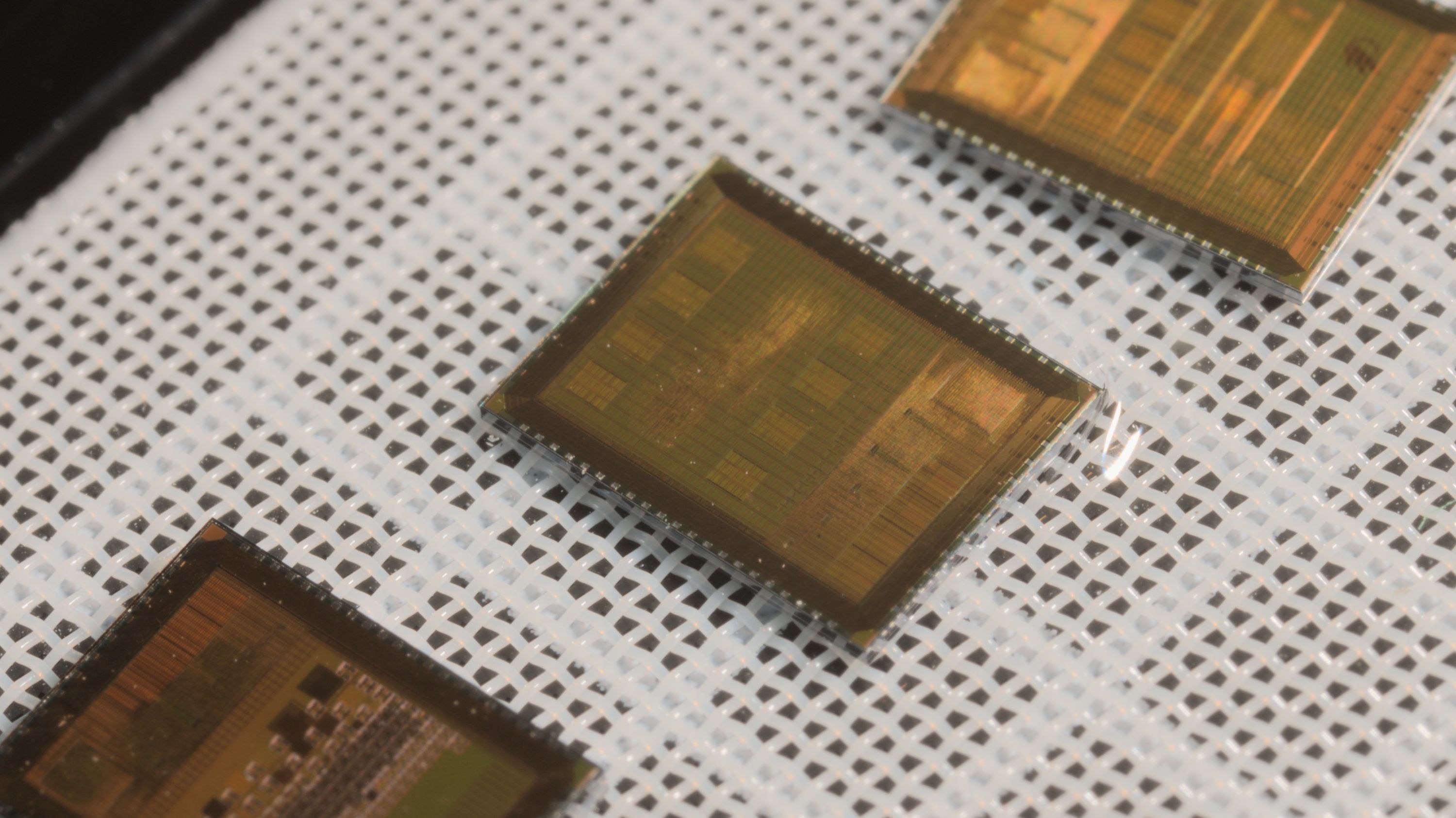
Get 1,000 custom silicon dies from as low as $2 per die with early bird pricing. wafer.space‘s third production run on GlobalFoundries’ GF180MCU 180 nm mixed-signal process is coming soon. Thanks to open PDKs, advancing open-source EDA, and programs like Tiny Tapeout, it has never been easier to design a chip. With wafer.space, you can turn a design into real, working chips. We provide pooled fabrication with clear specs, an automated submission system, and a shipment of real silicon you can hold, probe, and ship to other people.
Run 3 builds off of the successes we had in both Run 1 and Run 2. Many designs were submitted by universities, companies, hobbyists and community groups from around the world. Now we are doing it again, with another new slot size, better tooling, and lessons learned from our previous runs.
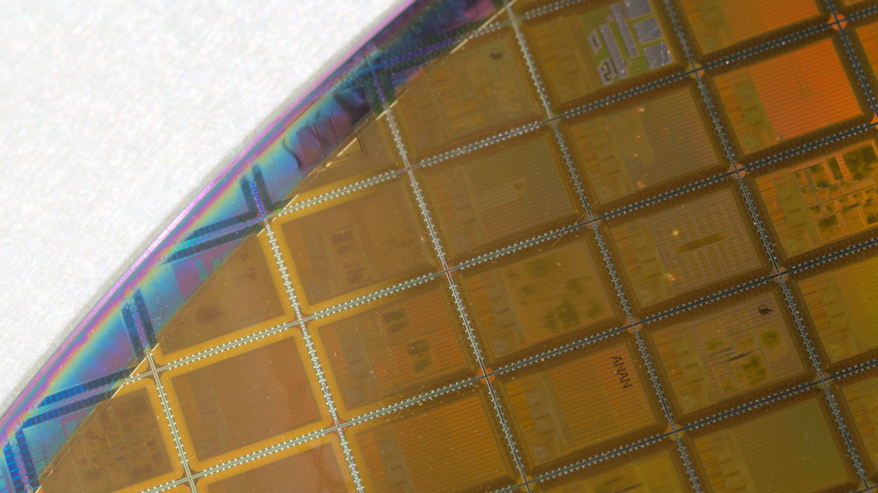
Orders were painful: opaque quotes, setup fees, big MOQs, long waits, and DIY panelization. Then pooling services like OSH Park fixed it with predictable pricing, frequent runs, and no-nonsense logistics. wafer.space brings that shift to silicon.
Run 3 introduces several improvements based on what we learned from shipping Run 1 & 2.
Quarter-sized slot: We’re adding another size option for Run 3. This tiny slot packs a punch with 4.9 mm² of silicon starting from just $2,000! Tapeout test structures, analog circuits, or compact digital designs without paying for silicon you do not need.
Further improvements to the toolchain: The submission platform has once again been updated to catch more issues, earlier, and faster. Bugfixes and stricter DRC mean you can be confident in your tapeout.
More examples: Run 1 contains 29 public designs, and Run 2 adds many more. These are real tapeouts which you can use to study and build upon. Projects vary from simple test structures to Linux-capable SoCs, covering digital, analog, and mixed-signal approaches.
The tools, ecosystem and community continue to evolve and grow with each run, but the flow has been proven. Real silicon
has been received by people across the world and you can explore some featured designs below.
Our first production run filled every slot on the reticle. Many designs from universities, companies, hobbyists, and community groups have been fabricated at GlobalFoundries. 29 of those projects have public repositories you can study right now.
Here are some highlights:
KianV: A 32-bit RISC-V SoC with SV32 MMU support, capable of running Linux and XV6. Complete with SDRAM controller, SPI, UART, GPIO, and a custom bring-up PCB.
FABulous FPGA: An open-source FPGA with 480 LUT4s, 6 SRAM blocks, 6 MACs, and 48 IOs, generated using the FABulous eFPGA framework and programmable via Yosys and nextpnr.
Z80 Open Silicon: A pin-compatible, open-source replacement for the classic Zilog Z80 8-bit CPU.
Tiny Tapeout GF: The Tiny Tapeout multi-project chip platform ported to GF180MCU, enabling dozens of small designs to share a single slot.
Racquet: A multi-core SoC based on the award-winning SERV RISC-V CPU, fitting up to 23 cores with local SRAM, inter-core communication queues, and a range of peripherals.
ISHI-KAI: A Japanese community project where 14 novice semiconductor designers each created analog circuits (inverters, op-amps, ADCs, PLLs, bandgap references) using xschem and KLayout.
RISCBoy-180: A video games console on a chip, with a RISC-V CPU, RISC-V APU, and custom graphics hardware.
FazyRV Hachure: A System-on-Chip integrating seven different variants of the bit-serial FazyRV RISC-V core in one chip for testing and research.
Browse the full list of public projects at github.com/wafer-space/ws-run1.
Run 2 is still in progress, but we have a couple to share!
FABulous FPGA: Back for Run 2, now with four times as much SRAM and much faster thanks to a community created standard cell library.
SRAM Macro: A selection of SRAMs for design validation, removing the hurdle of designing your own.
MPW by Avalon Semiconductors: Multi-project die containing various designs such as a replica 6502, a DRAM controller, NTSC test signal generator and more.
EuroSynth: A fully digital eurorack kitchen-sink synthesizer, containing a bank of isolated sound engines. Capable of streaming to an external DAC.
SlugTPU: An open-source tensor processing unit designed to accelerate quantized neural network inference. It features an 8x8 matrix multiply unit, a scalar post processing pipeline, 2 KiB SRAM data cache and a 256 byte instruction cache.
µTheia: An event-based machine vision ASIC for motion pattern classification. Uses EVT2 event streams, which are then decoded, compressed, sorted and computed. Detections can be reported through SPI or physical pins.
Run 3 offers four slot sizes. All sizes use the same GF180MCU process, the same padframe infrastructure, and the same submission platform. Every slot includes 1,000 dies.
| 1x1 (Full) | 0.5x1 (Half Width) | 1x0.5 (Half Height) | 0.5x0.5 (Quarter) | |
|---|---|---|---|---|
| Die Size | 3.93 mm x 5.12 mm | 1.94 mm x 5.12 mm | 3.93 mm x 2.53 mm | 1.94 mm x 2.53 mm |
| Die Area | 20.14 mm² | 9.92 mm² | 9.95 mm² | 4.90 mm² |
| Usable Silicon | 19.67 mm² | 9.55 mm² | 9.62 mm² | 4.67 mm² |
| Core Area | 12.92 mm² | 4.46 mm² | 5.02 mm² | 1.73 mm² |
| Default I/O Count | 56 | 56 | 56 | 48 |
| Default Total Pads | 74 | 72 | 72 | 56 |
| Early Bird Price | $7,000 ($7/die) | $4,000 ($4/die) | $4,000 ($4/die) | $2,000 ($2/die) |
| Standard Price | $8,000 ($8/die) | $5,000 ($5/die) | $5,000 ($5/die) | $3,000 ($3/die) |
Usable silicon is the die area minus the seal ring (~26 um each side). This is the area available when using a custom pad ring or no pad ring. Core area is the area inside the default pad ring.
For detailed slot specifications including padframe layouts and design constraints, see the slot size documentation.
Choosing a slot size: The 0.5x1 (half width) gives a tall, narrow die, ideal for I/O-heavy designs where signals concentrate along the long edges. The 1x0.5 (half height) gives a wide, short die, ideal for designs that benefit from a wider core. The 1x1 (full) provides maximum area for complex SoCs and mixed-signal designs. These three sizes share the same 56 I/O pad configuration, but the half-sized ones miss out on two extra power pads. New for this run, 0.5x0.5 (quarter) provides a smaller die at a much lower price point. Ideal for prototyping designs which don’t need the area offered by the other slots, but still just as capable as they all target GF180MCU. The quarter slot provides 48 I/O pads and 8 power pads.
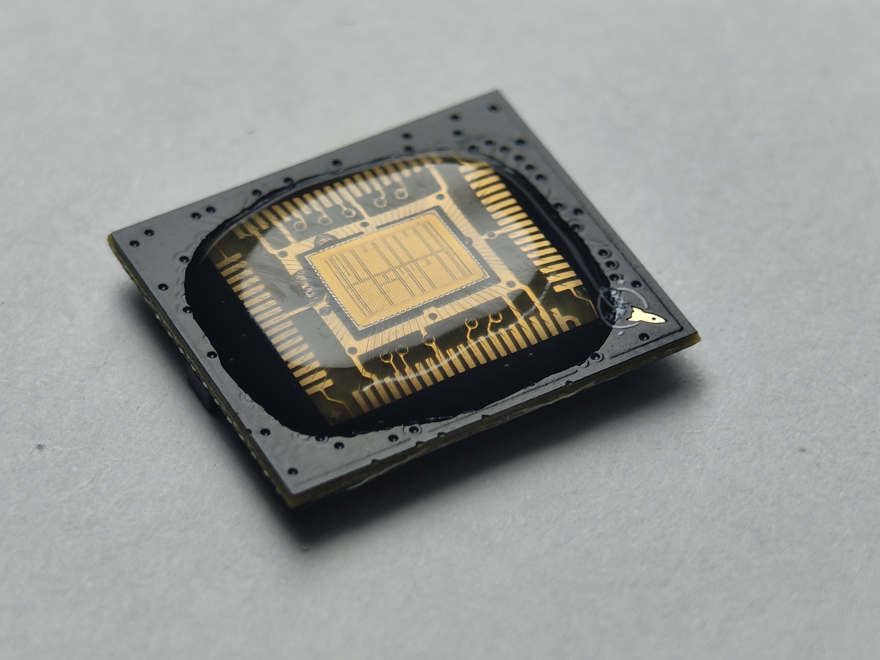
Receive your dies wire-bonded onto small PCBs, ready for testing and integration. Learn more about the process
in our progress update.
Add-on to any slot purchase. Costs $1,500 ($1.50/die).
The gf180mcu-project-template provides a ready-to-use starting point with LibreLane configuration, a Nix-based development environment, cocotb testbenches, and example designs. Clone it, drop in your Verilog, and run make librelane to go from RTL to GDS.
No. The PDK is open; your design can be open or closed.
The main changes are: a new smaller slot, stricter and more comprehensive DRC checking, an improved submission platform, and overall improvements to the toolchain. The process, foundry, and overall approach are the same.
It depends entirely on your design. For maximum core area, consider the 1x1 slot with its 12.92 mm² of core area. If your design is smaller, or is I/O heavy, then the half slots may offer a better shape for your design. If your design is even smaller, then the quarter slot offers
the lowest cost of entry. Check the slot size documentation for detailed comparisons.
No, but the community has created example pad rings and reviews of common pitfalls. The gf180mcu-project-template includes a default padframe configuration, and there are previous public designs you can use as references.
The full slot supports 56 I/O with 74 pads total. The half-sized slots also support 56 I/O, but total pad count is reduced to 72. The quarter-sized slot has 48 I/O with 56 pads total. The actual number you use depends on your pad pitch and die edge budget.
Yes. You own the full die area of your slot.
Absolutely. 29 public repositories from Run 1 are listed at github.com/wafer-space/ws-run1. Several of these include detailed documentation of their design process and decisions.
Fabricated on GF180MCU at GlobalFoundries in Singapore. Dicing and logistics via qualified partners. Final shipping from Singapore or our fulfillment partner.
You don’t have to wait for the campaign to begin to start creating your design.
If you need professional design help, several companies offer paid engineering services for GF180MCU designs. Options include full custom design, verification help, or guidance on a first tapeout. See the design help page for details.
Subscribe to be notified when Run 3 launches. In the meantime, you clone the project template and start designing right away.

· wafer.space · waferspacesg · wafer.space
wafer.space provides budget silicon manufacturing.